- +86-755-23012705
- Building 3, Jinfeng Industrial Park, Fuyong Street, Baoan District, Shenzhen ,China
- [email protected]
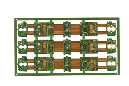
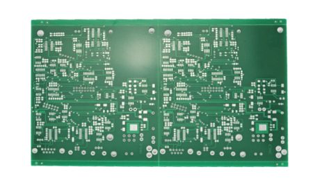
The circuit board on the PCB production line is the working board, after all the processes are printed, it needs to be divided into a small PCB board, which is efficient and fast when the circuit board is formed. Hollow lotus strips, in which the V-cut is used most for the regular board, the stamp hole is used more in the guide board, and the hollow connecting strip is connected in the board with a very narrow plate, such as some half-hole process circuit boards, the content of this chapter mainly explains in detail the following three puzzle methods and explains the difference between them!
Also known as “V-CUT”, is to draw a groove at the junction of the two boards, the connection of the board in this place is relatively thin and easy to break. And the edges of the two boards can be merged when the puzzle is made, in addition, the V cut is generally a straight line, and there will be no complex traces such as bending arcs. So you can try to be in a straight line when imposing, pay attention to leaving a gap between the two boards for the V-cut, generally 0.4mm can, and the V-cut line can be represented by using 2D lines in all layers.
Because the V cut can only go straight line, it is only suitable for the panel connection of the regular PCB board, for the irregular PCB board, such as the round one, you need to use the stamp hole to connect the panel.

It is another way of connecting the puzzle, generally used in the special-shaped plate, at the edge of the two boards through a small plate to connect, and this small plate and the connection of the two plates have many small holes, so easy to break, the reason why it is called “stamp hole”, because the edge of the board after breaking is like the edge of the stamp.
PCB stamp hole refers to a special hole located on the edge of the circuit board to fix and support the PCB board. Stamp holes usually consist of a pair of small holes that are connected to adjacent support points to provide a stronger holding force. This type of hole is common in PCB designs, especially in applications where circuit boards need to be mounted or connected.
The name stamp hole comes from its design that resembles a postage stamp. The design of the stamp holes allows the PCB board to be fixed more firmly on the chassis or frame and is not easy to bend or deform. The location and size of the stamp holes need to be designed according to the actual application to ensure the support and fixation of the PCB board.
The manufacture of stamp holes requires the use of specialized tools and techniques. During the production of circuit boards, stamp holes need to be drilled first, then sheet metal and pressed. The manufacture of stamp holes requires precise control and high-quality workmanship to ensure the accuracy and quality of the holes.

In PCB design, the design and layout of stamp holes need to take into account the overall structure and support needs of the PCB board. Designers need to arrange the stamp holes reasonably according to the actual application scenarios and mechanical structure requirements to ensure the fixation and stability of the circuit board.
The connection method is similar to the stamp hole, the difference is that the connecting part of the strip is narrower, and there is no vias on both sides. This way has a disadvantage that there will be an obvious bump after the board is broken, and the bump of the stamp hole is not very obvious because it is separated by the via, since this is why use this way? In fact, there is a situation where the stamp hole and V cut can not be used, that is, when the half-hole module is made all around, so it can only be connected at the four corners of the module through the hollow connecting strip.

Your Trusted Partner for PCB Success: XPCB Limited
Let XPCB Limited be your guide to PCB success. Our comprehensive PCB manufacturing, rapid prototyping, and turnkey PCBA services are designed to meet your needs with ease. Count on us to deliver reliable solutions that exceed your expectations. With XPCB Limited, your journey to PCB excellence starts here.


XPCB Limited is a premium PCB & PCBA manufacturer based in China.
We specialize in multilayer flexible circuits, rigid-flex PCB, HDI PCB, and Rogers PCB.
Quick-turn PCB prototyping is our specialty. Demanding project is our advantage.
Tel : +86-136-3163-3671
Fax : +86-755-2301 2705
Email : [email protected]
© 2024 - XPCB Limited All Right Reserve
