- +86-755-23012705
- Building 3, Jinfeng Industrial Park, Fuyong Street, Baoan District, Shenzhen ,China
- [email protected]
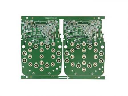
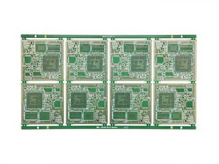
What does HDI circuit board mean: HDI circuit board is HDI (high-density interconnection) PCB, which is a kind of (technology) for the production of PCBs, and a PCB with high circuit distribution density using micro-blind and buried via technology.
With the development of the design of portable products in the direction of miniaturization and high density, the design of PCBs is becoming more and more difficult, which puts forward higher requirements for the PCB production process. At present, most of the portable products make the BGA package with a pitch of less than 0.65mm, and the blind and buried via design process is used, so what is the blind and buried via PCB?
Blind and buried PCBs, also known as “HDI boards”, are often used in the application of high-end products such as mobile phones, GPS navigation, etc.
PCB holes are divided into three types: blind vias, buried vias, and through vias, among which: blind vias are the type of vias that connect the inner traces of the PCB with the traces of the surface of the PCB, and this hole does not penetrate the entire board. Buried vias are only connected to the via type of the traces between the inner layers, so they are not visible from the surface of the PCB. A through hole is a hole that can be seen directly from the top layer to the bottom layer, which is called a “through hole”. Blind and buried via PCBs

When it comes to blind/buried PCBs, the first thing that comes to mind is the high multi-layer board, which consists of an inner circuit and an outer circuit, and then uses drilling and the process of metallization in the hole to achieve the internal connection function of each layer of the circuit. However, due to the increase of line density and the continuous updating of the packaging method of the parts, in order to allow more and higher performance parts to be placed in the limited PCB area.
In addition to the finer line width, the aperture has also been reduced from 1 mm in the DIP hole diameter to 0.6 mm in the SMD, and further reduced to less than 0.4mm. However, it still occupies the surface area, so there are buried and blind vias, which are defined as follows:

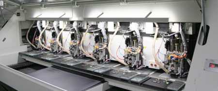
There are three different ways to make a blind well plate, as described below:

Simplify Your PCB Journey with XPCB Limited
XPCB Limited simplifies the PCB process for you. With our quick-turnaround prototyping and turnkey PCBA services, we ensure that your projects move forward smoothly and efficiently. Trust our commitment to quality and timeliness as we help you bring your designs to life. Choose XPCB Limited for a hassle-free PCB experience.


XPCB Limited is a premium PCB & PCBA manufacturer based in China.
We specialize in multilayer flexible circuits, rigid-flex PCB, HDI PCB, and Rogers PCB.
Quick-turn PCB prototyping is our specialty. Demanding project is our advantage.
Tel : +86-136-3163-3671
Fax : +86-755-2301 2705
Email : [email protected]
© 2024 - XPCB Limited All Right Reserve
