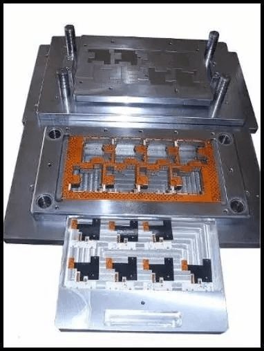
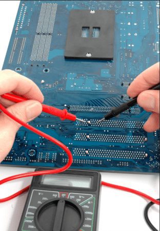
For manufacturers specializing in the production of circuit boards, low-volume board flying probe testing is an indispensable step. Large quantities of boards will normally choose to open the test rack. Because after all, the price of the flying probe test needs to be prepaid every time, and the test rack only needs to be paid once, and there is no need to pay additional test fees for subsequent tests.
So what does the flying probe test mean?PCB flying probe test is one of the methods to check the electrical function of the PCB. The principle of the flying probe tester is a system for testing PCBs in a manufacturing environment, using four to eight independently controlled probes that move to the components under test and are transported to the testing machine via a belt or other UUT conveyor system.
The probes of the tester test the individual components of the UUT by contacting the test pads and vias, and the test probes are connected to the drivers (signal generators, power supplies, etc.) and sensors (digital multimeters, frequency counters, etc.) through a multiplexing system to test the components on the UUT. While one component is being tested, the other components on the UUT are electrically shielded by a probe to prevent interference with the readings.
Import the layer files processed by the engineering department, check, arrange, align, change the two outer lines to fronrear respectively, and rename the inner layer to ily02, ily03, ily04neg (if negative), rear, rearmneg.
Add three layers, copy and paste the two solder mask layers and drilling layers to the new three layers, and rename them to fronmneg, rearmneg, mehole, and then change the two layers of fronmneg and rearmneg that have just copied the past to the round with D code of 8mil We call fronmneg the front layer test point, and rearmneg the back test point.
Delete the NPTH hole and find out the location of the via hole against the line.
Take the fron, mehole layer as the reference layer, and the fronmneg layer is renamed ON for detection, check whether the test points are at the opening of the front layer line, the test points in the holes greater than 100mil need to be weighed and moved to the weld ring for testing, and the test points at the BGA that are too precise should be dislocated for testing, and the back layer should be operated in the same way.

Copy the sorted test point fronmneg to the fron layer, copy the rearmneg to the rear layer, and activate all the layers, moving to 10,10mm. Then name the output gerber file as fron, ily02, ily03, ily04neg, ilyo5neg, rear, fronmneg, rearmneg, meholemet01-02, met02-09, met09-met10 layers.
Use CAM software to export all gerber files fron, ily02, ily03, ily04neg, ilyo5neg, rear, fronmneg, rearmneg, meholemet01-02, met02-09, met09- met10 layers, press netannotati onof The artwork key generates the network, press the maketestprograms key to generate the test document, enter the non-pore D code, and finally test the datum point to complete and save, and place the PCB board on the flying probe testing machine to start the test.
Discover a World of Possibilities with XPCB Limited
At XPCB Limited, we’re here to help you explore new horizons. Our advanced PCB manufacturing, rapid prototyping, and turnkey PCBA solutions make it easy for you to turn your ideas into reality. Trust us to deliver excellence and reliability every step of the way. Join us and experience the power of innovation with XPCB Limited by your side.


XPCB Limited is a premium PCB & PCBA manufacturer based in China.
We specialize in multilayer flexible circuits, rigid-flex PCB, HDI PCB, and Rogers PCB.
Quick-turn PCB prototyping is our specialty. Demanding project is our advantage.
Tel : +86-136-3163-3671
Fax : +86-755-2301 2705
Email : info@x-pcb.com
© 2024 - XPCB Limited All Right Reserve