- +86-755-23012705
- Building 3, Jinfeng Industrial Park, Fuyong Street, Baoan District, Shenzhen ,China
- [email protected]
High-Density Interconnect (HDI) PCBs have revolutionized the electronics industry, enabling the design of compact and highly functional devices. With their intricate layers and advanced manufacturing techniques, HDI PCBs offer several advantages, including reduced size, improved performance, and enhanced electrical connectivity. However, the assembly of HDI PCBs presents unique challenges that manufacturers must navigate to ensure product reliability and performance. This blog will explore these challenges and discuss potential solutions.
One of the defining features of HDI PCBs is the use of microvias—small holes that connect different layers of the circuit board. These microvias can be blind or buried, allowing for greater design flexibility but also introducing complexities in manufacturing.
Challenge: The drilling and plating of microvias require precise control to avoid defects such as fractures or blockages. Traditional drilling methods may not suffice for the tiny dimensions of these vias.
Solution: Employing advanced laser drilling technology can enhance precision and minimize damage. Additionally, rigorous inspection methods should be implemented to ensure the integrity of the microvias throughout the manufacturing process.
HDI PCBs often require specialized materials that can handle high frequencies and thermal stresses. The choice of substrate material directly affects the board’s performance.
Challenge: Selecting materials that meet both electrical performance and thermal management requirements can be difficult. Inadequate material choices may lead to signal integrity issues or reduced lifespan of the PCB.
Solution: Collaborating closely with material suppliers can help manufacturers choose the right materials. Conducting thorough testing on selected substrates can also ensure they meet the necessary specifications before assembly.

The compact nature of HDI PCBs means that components are densely packed, making soldering and placement more complicated.
Challenge: With limited space, ensuring accurate component placement and achieving high-quality solder joints becomes more difficult. Issues like bridging, insufficient solder, or cold joints can arise, impacting the overall reliability of the assembly.
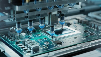
Solution: Utilizing automated pick-and-place machines can enhance placement accuracy. Additionally, employing advanced soldering techniques, such as selective soldering or reflow soldering, can improve joint quality and reduce defects.
As electronic devices become more powerful, managing heat dissipation in HDI PCBs is crucial for maintaining performance and reliability.
Challenge: The increased density of components can lead to higher temperatures, risking thermal failure and performance degradation.
Solution: Designing for thermal management from the outset is essential. This can include incorporating thermal vias, using heat sinks, or selecting materials with good thermal conductivity to ensure efficient heat dissipation.
Due to the complex nature of HDI PCBs, traditional testing methods may not effectively identify issues.
Challenge: The compact layout and intricate designs make it challenging to perform thorough testing. Many defects may go undetected until the final product fails.
Solution: Implementing advanced testing techniques, such as automated optical inspection (AOI) and X-ray inspection, can help detect defects early in the assembly process. Functional testing should also be conducted to verify that the assembled PCB meets performance specifications.

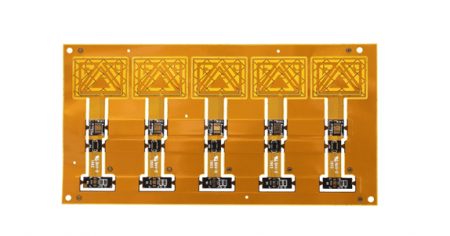
4 layer Flex Circuit with HDI
The complexity of HDI PCB assembly necessitates stringent process control to ensure quality.
Challenge: Variability in manufacturing processes can lead to inconsistencies and defects, which may not be apparent until later in the production cycle.
Solution: Establishing robust process controls and quality assurance protocols is vital. Regular training for staff and implementing real-time monitoring systems can help maintain quality throughout the assembly process.
Assembling HDI PCBs presents unique challenges that require careful consideration and advanced techniques. By addressing issues related to microvia technology, material selection, soldering, thermal management, testing, and process control, manufacturers can enhance the reliability and performance of HDI PCBs. As the demand for smaller, more powerful electronic devices continues to grow, overcoming these challenges will be essential for staying competitive in the rapidly evolving electronics landscape. Through innovation and collaboration, the industry can ensure that HDI PCBs remain a cornerstone of modern electronics design and manufacturing.
Take Your Projects to New Heights with XPCB Limited
XPCB Limited offers top-notch PCB manufacturing, quick-turnaround prototyping, and turnkey PCBA services designed to make your projects shine. Count on us to bring your ideas to life with efficiency and quality. Your success matters to us, and we’re here to make your innovation journey smooth and rewarding.


XPCB Limited is a premium PCB & PCBA manufacturer based in China.
We specialize in multilayer flexible circuits, rigid-flex PCB, HDI PCB, and Rogers PCB.
Quick-turn PCB prototyping is our specialty. Demanding project is our advantage.
Tel : +86-136-3163-3671
Fax : +86-755-2301 2705
Email : [email protected]
© 2024 - XPCB Limited All Right Reserve
