
ATE PCB Manufacturing Service
Advanced ATE Board Solutions
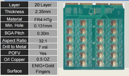
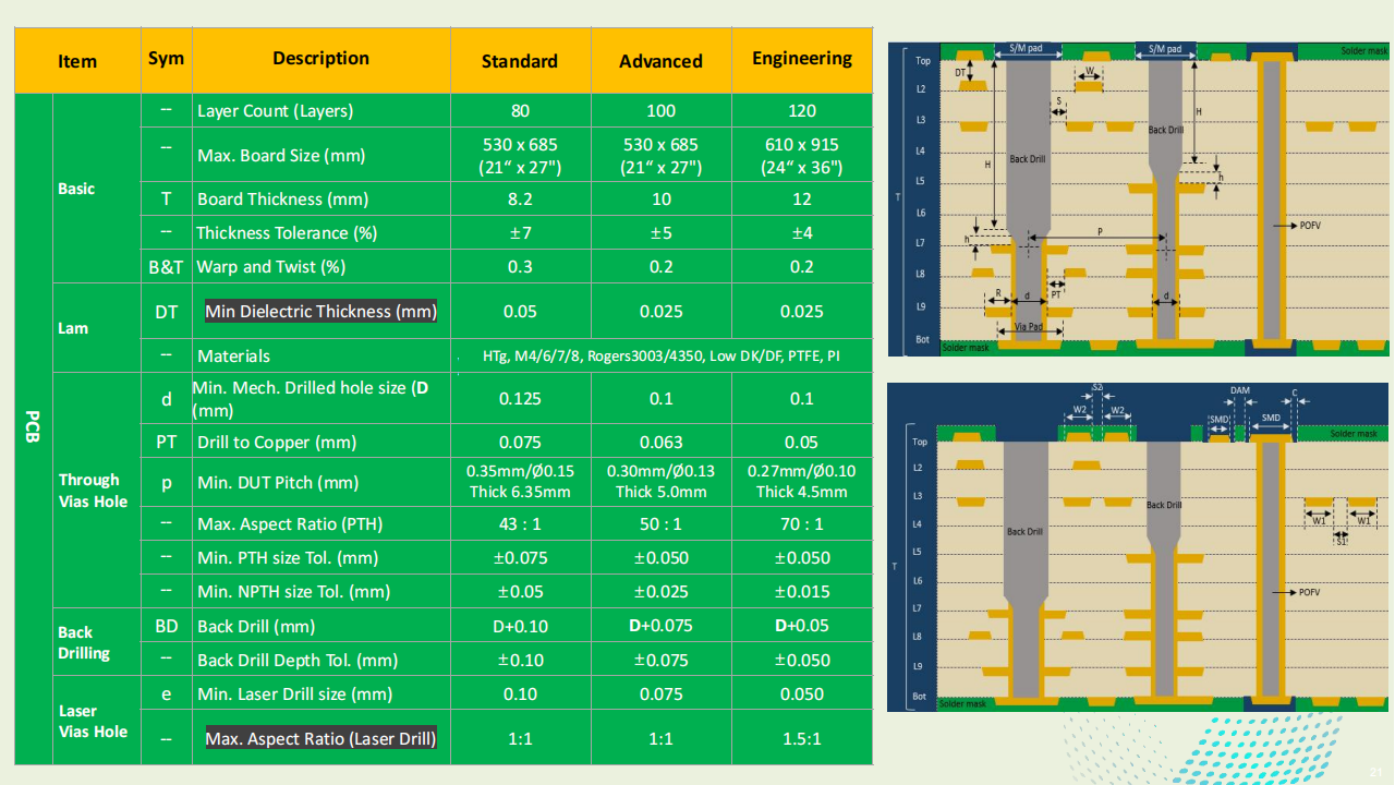
XPCB delivers high-performance ATE PCBs engineered for the most demanding test environments. Our advanced capabilities, including precise POFV (Plated Over Filled Via) technology, back drilling for enhanced signal integrity, HDI (High-Density Interconnect) fabrication on any layer, and support for fine pitch components and trace widths with aspect ratios up to 40:1, ensure your complex designs are flawlessly executed.
- MLO/Interposer Series
- Probe Card Series
- Load Board Series
- BIB Series
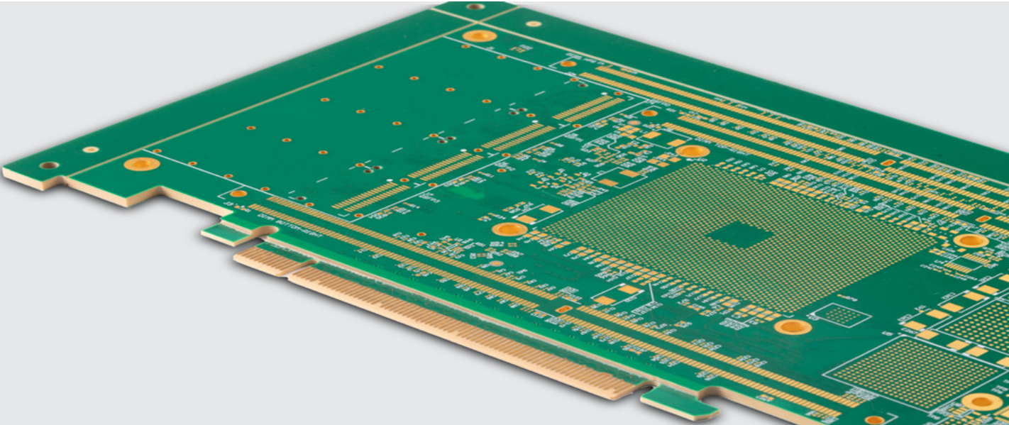
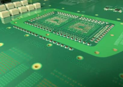
- MLO Series
- Probe Card
- Load Board
- BIB Series
The MLO or Interposer is a critical interface PCB in automated test equipment (ATE). It acts as the central connection hub, routing signals and power between the tester and the device under test (DUT). The interposer, often a subset of the MLO, specifically adapts the probe card’s connection points to the DUT, especially crucial for fine-pitch components or complex packaging.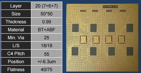
Probe Card PCB houses an array of microscopic probes (needles or membrane contacts) that make direct electrical contact with the DUT’s pads or bumps. It’s the physical interface that allows the tester to send signals to and receive signals from the chip. 
Load boards are used to electrically tests individual integrated circuits (ICs), selecting only those that meet predefined quality standards. These ICs, often using Ball Grid Array (BGA) packaging with pitches typically 0.35mm or larger, require load boards with precise impedance control for accurate testing. The ICs themselves are manufactured from silicon wafers through a series of steps: die sawing, die bonding, wire bonding, and finally encapsulation in a protective material like epoxy resin.

Burn-In Board tests the long-term reliability of packaged integrated circuits (ICs) by subjecting them to a controlled aging process over a specific period.
Conquer Your Complex ATE Challenges
Expert solutions for high-density and high-speed ATE PCB fabrication. Get a quote today!
Get QuoteATE PCB Process Capability
ATE PCB PROJECTs
LEO Satellite Communication 16x16 Phased Array
26L Probe_Card PCB
60L 93K Loadboad
20L DUT 5.5mm
Image Accordion #1
Image Accordion Content Goes Here! Click edit button to change this text.
42L RF Load board
ATE PCB SMT
18L Loadboard HALF
Accordion content goes here!
Our ATE PCB Equipment
AOI Equipment
Inner Layer DES Development and Etching Strip Line
CCD Drilling
Copper Reduction Line
SES Strip and Etch Tin Line
Are you facing challenges in finding reliable and high-performance ATE PCBs for your complex testing needs? XPCB specializes in delivering cutting-edge printed circuit board solutions tailored specifically for Automated Test Equipment (ATE) applications. Our advanced fabrication capabilities ensure precise and efficient testing for a variety of industries, including semiconductor, automotive, medical, and aerospace.
What sets XPCB’s ATE PCB solutions apart?
Advanced Technologies: We leverage the latest technologies to produce high-quality PCBs that meet the stringent demands of ATE. Our expertise includes:
- POFV (Plated Over Filled Via): Ensures superior reliability and thermal management for high-power applications.
- Back Drilling: Eliminates stub lengths and optimizes signal integrity for high-speed designs.
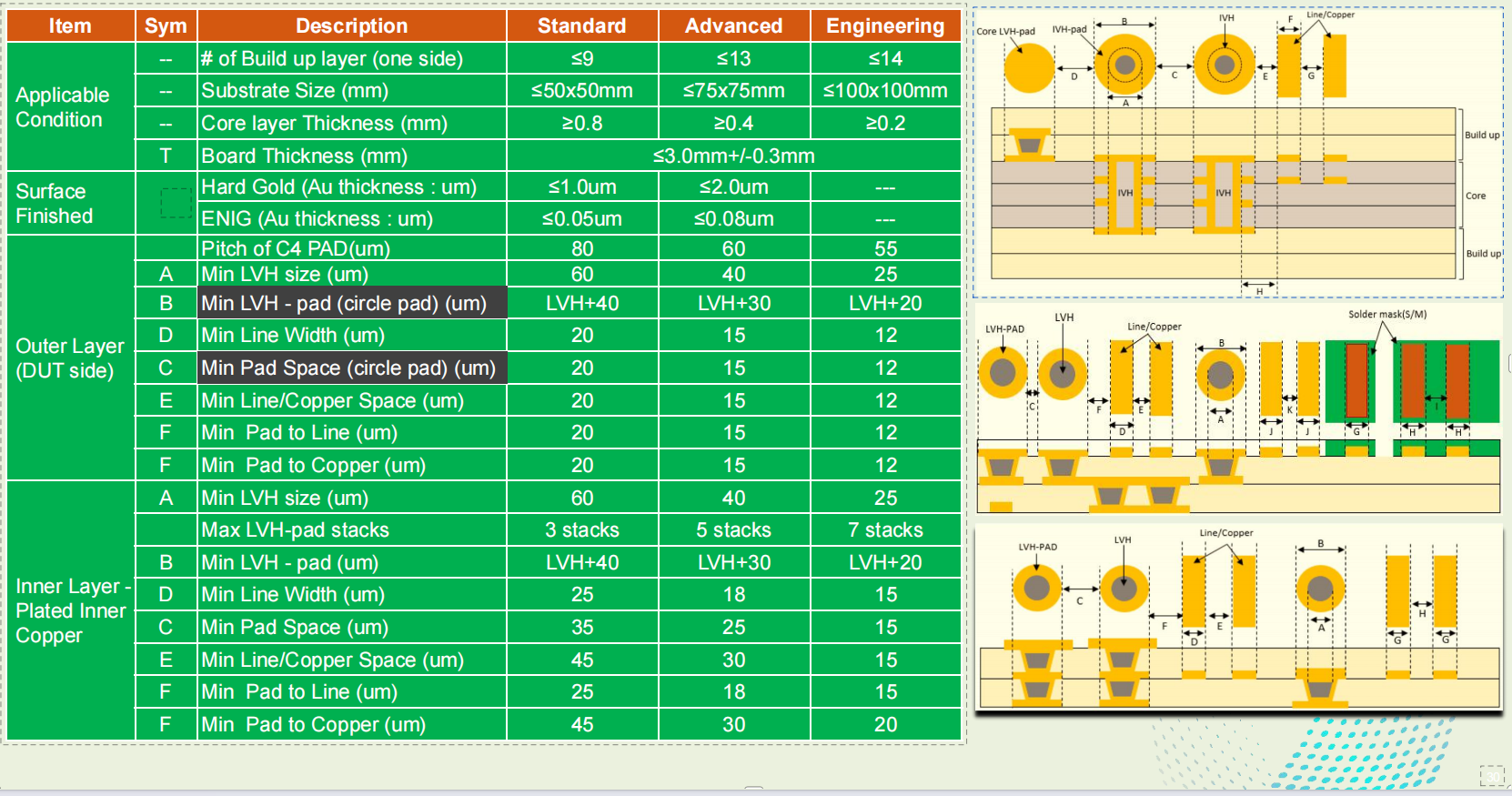
- HDI (High-Density Interconnect) Any Layer: Enables complex routing and miniaturization for space-constrained designs.
- Fine Pitch and Line Capabilities: Supports fine-pitch components and intricate trace routing for increased density and performance.
- 40:1 Aspect Ratio: Allows for smaller vias and denser circuitry, crucial for advanced ATE designs.
Industry Expertise: We understand the unique challenges of various industries and provide tailored solutions to meet specific requirements. Our experience spans:
- Semiconductor Testing: High-speed, high-density PCBs for wafer testing, chip packaging, and final product testing.
- Automotive Electronics Testing: Robust and reliable PCBs for testing ECUs, sensors, and other critical components.
- Medical Device Testing: Precise and biocompatible PCBs for testing medical devices with stringent quality standards.
- Aerospace and Defense Testing: High-reliability PCBs designed to withstand harsh environments and meet stringent industry standards.
Rapid Prototyping and Production: We offer quick-turn prototyping services to accelerate your development cycles and flexible volume production to meet your scaling needs.
Expert Engineering Support: Our experienced engineers provide Design for Manufacturability (DFM) feedback and dedicated support throughout your project lifecycle.


