- +86-755-23012705
- Building 3, Jinfeng Industrial Park, Fuyong Street, Baoan District, Shenzhen ,China
- [email protected]
In the world of electronics, ensuring the reliability and functionality of Printed Circuit Board Assemblies (PCBAs) is essential for the overall performance of a product. Since PCBA is the heart of most electronic devices, it must undergo rigorous testing to ensure that every component is properly placed, soldered, and electrically functional. There are several common testing methods used in the industry to check the quality and integrity of PCBA. In this blog, we will explore these methods and their significance in the manufacturing process.
Visual inspection is one of the most basic and widely used testing methods in PCBA production. It involves manually or automatically inspecting the surface of the circuit board for visible defects.
This can include issues such as:
Soldering defects (cold solder joints, excess solder, or poor soldering quality)
Component misplacement (components installed incorrectly or upside down)
Board defects (missing components, damaged pads, or traces)
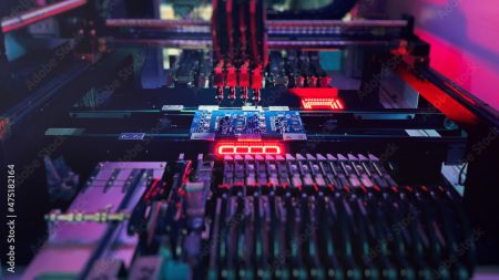
Modern manufacturing lines often utilize Automatic Optical Inspection (AOI) machines, which use high-resolution cameras and software to automatically scan the board for any defects. AOI provides a quick and efficient way to catch defects early in the production process.

Quick and cost-effective for detecting visible defects.
AOI systems can detect even the smallest issues with high precision.
Limited in detecting internal defects like those under large components or solder joints in BGA (Ball Grid Array) packages.
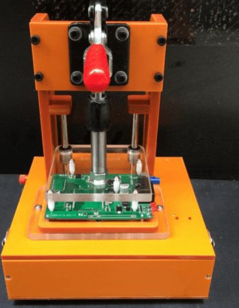
Flying Probe Testing is an electrical testing method that uses a set of movable probes to check the electrical continuity and connections on the PCBA. Unlike traditional in-circuit testing (ICT), FPT does not require any custom-made test fixtures, making it highly flexible for low to medium-volume production. The probes touch specific test points on the board and check for open circuits, shorts, or incorrect connections.
Ideal for small production runs or prototype testing.
No need for custom test fixtures, making setup faster and more affordable.
Slower testing speed compared to other methods like ICT.
Not suitable for high-volume production due to slower throughput.

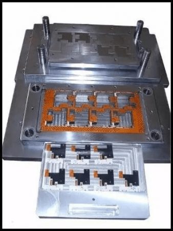
In-Circuit Testing is one of the most widely used methods in PCBA testing, especially for mass production. ICT uses specialized test fixtures and probes to check for open circuits, short circuits, component values, and correct component placement. It can also check for component faults such as incorrect or missing components.
High-speed, precise electrical testing.
Able to detect a wide range of defects, including shorts, opens, and incorrect component values.
Requires the creation of custom test fixtures, which adds to the initial setup cost.
Not suitable for testing high-density boards with many fine-pitch components like BGAs.
Automated Optical Inspection (AOI) uses high-resolution cameras to capture detailed images of the PCBA and analyze them for defects. AOI systems can detect:
Soldering defects (like bridges or voids in solder joints)
Component alignment and placement issues
Missing components or wrong parts
AOI is particularly useful in high-volume production environments, where quick and accurate inspections are necessary.
Fast and efficient, ideal for high-volume manufacturing.
Can detect even minor soldering defects and component placement issues.
Cons:
Limited in detecting internal defects (such as those in BGAs).
False positives may occur if the system is not properly calibrated.
5. X-Ray Inspection
X-ray inspection is a non-destructive testing method that allows engineers to examine the internal structure of PCBA, especially the solder joints under BGAs and other hidden components. Since X-rays can penetrate through the layers of the board, this technique can reveal soldering defects, such as cold joints, voids, and misalignments that are not visible externally.
Can detect hidden soldering defects, especially under BGAs or other large components.
Provides high-resolution images of the internal structures of the PCBA.
Expensive equipment and operating costs.
Requires specialized personnel to operate the system and interpret the results.
Functional testing checks whether the PCBA performs its intended functions. This is done by applying voltage to the circuit and using a test system to simulate the operating environment. Functional tests are often used to ensure that all components are working properly, such as checking that microcontrollers communicate with peripheral devices or that power supplies provide the correct output.

Validates the actual functionality of the PCBA, ensuring that it meets the specifications.
Can detect issues that may not be visible in other tests, such as software-related bugs or component interactions.
Time-consuming and requires a fully functional test setup.
Higher costs, especially if the product requires complex testing procedures.
Burn-in testing involves running the PCBA under elevated temperature and voltage conditions for an extended period. This is done to detect early failures or weak components that may fail later in the product’s lifecycle. It is commonly used in high-reliability industries like aerospace, medical devices, and automotive electronics.
Helps identify reliability issues before the product reaches the customer.
Reduces the likelihood of failures during real-world use.
Long testing periods can add significant production time.
May require additional equipment and resources for heat chambers or load simulators.
Each of these testing methods serves a unique purpose in ensuring the quality and reliability of PCBA. The choice of testing method depends on various factors, including the complexity of the PCBA, the production volume, and the required testing accuracy. A combination of visual inspection, electrical testing, and advanced techniques like X-ray inspection or functional testing is often used to ensure that every PCBA meets the highest quality standards before it is integrated into the final product.
By implementing these testing methods, manufacturers can significantly reduce the risk of defects, enhance product reliability, and ultimately deliver high-quality electronic devices to the market.
Discover a World of Possibilities with XPCB Limited
At XPCB Limited, we’re here to help you explore new horizons. Our advanced PCB manufacturing, rapid prototyping, and turnkey PCBA solutions make it easy for you to turn your ideas into reality. Trust us to deliver excellence and reliability every step of the way. Join us and experience the power of innovation with XPCB Limited by your side.


XPCB Limited is a premium PCB & PCBA manufacturer based in China.
We specialize in multilayer flexible circuits, rigid-flex PCB, HDI PCB, and Rogers PCB.
Quick-turn PCB prototyping is our specialty. Demanding project is our advantage.
Tel : +86-136-3163-3671
Fax : +86-755-2301 2705
Email : [email protected]
© 2024 - XPCB Limited All Right Reserve
