- +86-755-23012705
- Building 3, Jinfeng Industrial Park, Fuyong Street, Baoan District, Shenzhen ,China
- [email protected]
Surface Mount Devices (SMD) have become the backbone of modern electronic manufacturing, offering significant advantages such as compact size, high assembly density, and cost efficiency. The production process of SMDs is a highly automated and precise sequence of steps that ensures components are correctly placed, soldered, and tested before they are integrated into final electronic products. In this blog, we will take a deep dive into the typical production process of SMDs, from initial design and component selection to assembly and final inspection.
The first step in the production of SMDs is the design phase, where engineers design the circuit and choose the appropriate components. This stage involves the selection of the right SMD packages for various components, such as resistors, capacitors, integrated circuits (ICs), and transistors, based on the needs of the specific application.
Functionality: The components must meet the functional requirements of the circuit, such as signal processing, power management, or amplification.
Size and Package Type: The size of the SMD components is selected based on the available PCB space. The most common SMD package sizes include 0603, 0805, and 1206 for resistors and capacitors, while more complex ICs might come in QFN or BGA packages.
Electrical and Mechanical Characteristics: The voltage ratings, current handling capacity, and thermal properties of the components must match the application requirements.
Once the components are chosen, the schematic and layout of the printed circuit board (PCB) are created using specialized design software, which helps define where each component will be placed on the PCB.

After the design phase, the next step is the manufacturing of the PCB itself. The PCB serves as the platform where SMD components will be mounted. The process involves several key stages:
Material Preparation: The base material, typically made from copper-clad laminate, is prepared by applying a thin layer of copper on both sides.
Circuit Pattern Creation: Using a process called photolithography, the circuit pattern is transferred to the PCB. This involves coating the PCB with a photosensitive material, exposing it to light, and then developing the pattern of traces and pads that will connect the components.
Etching: The PCB is etched to remove the unwanted copper, leaving behind the necessary electrical traces for connections between the components.
Drilling (for vias): If necessary, small holes (vias) are drilled to allow electrical connections between different layers of a multi-layer PCB.
Once the basic PCB is fabricated, it undergoes further processes such as surface finishing (to protect the copper traces) and applying solder mask and silkscreen for labeling.
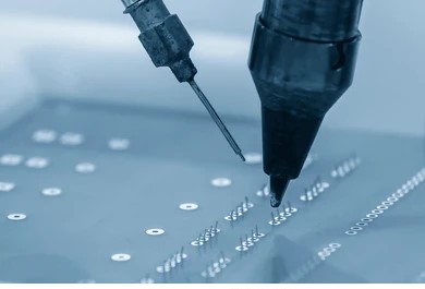
Solder paste is a critical element in the assembly of SMD components. It is a mixture of tiny solder balls suspended in flux, which allows components to be securely attached to the PCB during the soldering process. The solder paste is applied to the PCB in a precise manner to ensure that only the pads for the components are coated.
Steps in Solder Paste Application:
Stencil Printing: A metal stencil is used to apply the solder paste to the PCB. The stencil is aligned over the PCB, and the paste is spread over the surface using a squeegee, depositing the paste only on the areas where the components will be mounted.
Inspection: After the paste is applied, the PCB is inspected for accuracy. Automated optical inspection (AOI) systems are often used to ensure that the correct amount of solder paste has been applied to the correct locations.
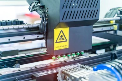
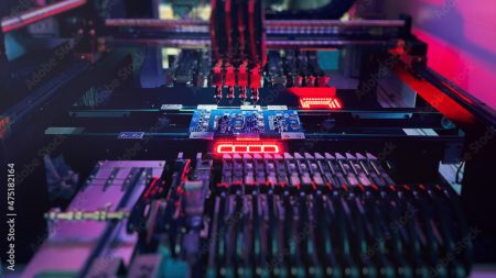
After solder paste application, the next step is placing the SMD components onto the PCB. This step is performed using automated pick-and-place machines, which are designed to precisely position components on the board.
Key Elements of Component Placement:
Automated Pick-and-Place Machines: These machines use suction or vacuum systems to pick up each component from a reel or tray and place it accurately onto the solder paste on the PCB. The placement accuracy is critical for ensuring that the components are aligned properly with the pads.
Component Orientation: For many SMD components, the correct orientation is crucial for functionality. The pick-and-place machine must ensure that the components are oriented properly (e.g., for ICs or diodes).
Modern pick-and-place machines are highly advanced, with high-speed capabilities that can place thousands of components per hour with high accuracy, ensuring fast and efficient production.

After the components are placed on the PCB, the next step is reflow soldering, where the solder paste is melted to create permanent electrical connections between the component leads and the PCB pads.
Reflow Soldering Process:
Preheating: The PCB is gradually heated to a temperature where the solder paste begins to liquefy. This step ensures that the components and PCB are gradually heated without thermal shock.
Reflow Stage: The temperature is raised to the melting point of the solder (usually around 220°C), causing the solder paste to reflow and form a solid bond between the components and the PCB.
Cooling: The PCB is then cooled, solidifying the solder joints and ensuring that the components are securely attached.
Reflow soldering is highly automated and ensures precise control over the soldering process, reducing the likelihood of defects such as cold solder joints, solder bridges, or component misalignment.
Once the components are soldered onto the PCB, the next step is inspection and testing. The goal is to ensure that the assembly is free from defects and that the components are functioning correctly.
Automated Optical Inspection (AOI): AOI systems use cameras and software to visually inspect the solder joints, component placement, and alignment on the PCB. This ensures that there are no visible defects such as solder bridges, misaligned components, or missing parts.
X-ray Inspection: For more complex components, such as BGAs (Ball Grid Arrays), which have hidden solder joints, X-ray inspection is used to verify the integrity of the solder joints.
Functional Testing: Functional tests are performed to verify that the PCB is operating as intended. This may involve checking the electrical signals, voltage levels, and functionality of various components.
In-Circuit Testing (ICT): This type of testing involves checking each component on the PCB for functionality by applying test points and verifying that the correct voltage and current are present.

Once the PCB passes inspection and testing, it is ready for final assembly. This may include additional components such as connectors, heat sinks, or mechanical enclosures. After assembly, the product is packaged for shipment, ensuring it is protected during transport and handling.
Conclusion The production process of SMD packaging is a complex, multi-step process that requires precision and attention to detail at every stage. From initial design and component selection to PCB manufacturing, solder paste application, component placement, and final inspection, each step plays a critical role in ensuring that the final product is of high quality. The automation of many of these steps has made SMD assembly fast, cost-effective, and highly scalable, enabling the mass production of modern electronic devices that are smaller, more efficient, and more powerful than ever before.
Make Your PCB Dreams a Reality with XPCB Limited
XPCB Limited is your go-to partner for turning your PCB dreams into reality. Our streamlined PCB manufacturing process, combined with quick-turnaround prototyping and turnkey PCBA services, ensures that your projects come to life with ease. Trust in our expertise and dedication to quality as we help you achieve your PCB goals. Join us and experience the difference with XPCB Limited.


XPCB Limited is a premium PCB & PCBA manufacturer based in China.
We specialize in multilayer flexible circuits, rigid-flex PCB, HDI PCB, and Rogers PCB.
Quick-turn PCB prototyping is our specialty. Demanding project is our advantage.
Tel : +86-136-3163-3671
Fax : +86-755-2301 2705
Email : [email protected]
© 2024 - XPCB Limited All Right Reserve
