- +86-755-23012705
- Building 3, Jinfeng Industrial Park, Fuyong Street, Baoan District, Shenzhen ,China
- [email protected]
Printed Circuit Boards (PCBs) are the backbone of modern electronics, connecting and powering everything from the most basic gadgets to advanced technologies like smartphones, wearables, medical devices, and automotive systems. As electronic devices continue to shrink in size and grow in functionality, PCB prototyping has evolved significantly. What started with simple designs in the early days of electronics has transformed into the ability to create complex, high-density interconnect (HDI) PCBs that are integral to the cutting-edge devices of today and tomorrow.
In this blog, we’ll explore the evolution of PCB prototyping, from the early days of simple single-layer boards to the advanced multi-layer, high-density designs used in the most complex applications today.
In the early days of electronics, PCB prototyping was a relatively straightforward process. The designs were simple, often involving just a single-layer board with a limited number of components. These early PCBs were primarily used in analog systems or early digital devices where complex routing and high-speed signals were not a concern.
The process for creating these early PCBs involved manual drafting of circuit layouts, followed by the creation of the copper traces that would form the connections between components. The boards were relatively large, and the components used were bulky and through-hole based, meaning they were inserted into holes drilled through the PCB. This simplicity made early PCB prototyping affordable and relatively quick but limited the complexity and performance of the final devices.
As technologies advanced, the need for more complex designs arose, and the first steps toward multi-layered boards began. Automated design tools like CAD (Computer-Aided Design) systems allowed for better precision and faster iterations, while drilling machines became more accurate, allowing manufacturers to create more intricate board layouts.

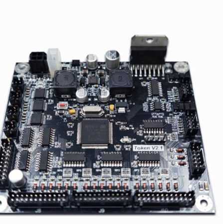
As digital electronics grew in sophistication, so did the complexity of PCB designs. Multi-layer PCBs—which feature multiple layers of copper traces separated by insulating material—began to emerge as a solution to handle the increasing number of components required for modern devices. Multi-layered boards allowed designers to stack circuit layers, significantly increasing the board’s density and functionality.
This evolution marked a major shift in PCB prototyping. CAD tools became more advanced, allowing designers to lay out more complex designs with finer detail. The number of layers in a PCB could now range from two layers to eight or more, each layer supporting different signal routes, power distribution, and ground planes. Multi-layer designs also enabled higher signal integrity and faster data transfer speeds, which were necessary for devices like computers, televisions, and early mobile phones.
As the technology behind multi-layer PCBs advanced, manufacturers began introducing more automated processes, such as laser drilling and automated assembly to streamline production. This reduced human error and increased efficiency in the prototyping process. However, despite these advancements, multi-layer boards still had certain limitations when it came to component density, particularly in devices with very small form factors.
The Emergence of HDI (High-Density Interconnect) PCBs
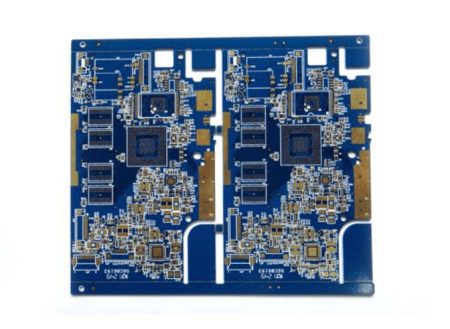
In recent years, the demand for smaller, more powerful electronic devices has accelerated the shift towards High-Density Interconnect (HDI) PCBs. These PCBs are designed to handle high-density layouts with microvias, fine-pitch components, and multi-layer configurations that enable significantly more complex designs than standard multi-layer PCBs.
HDI PCBs use microvias (tiny holes drilled using lasers) to interconnect the different layers of the board, as opposed to traditional vias, which are relatively large. This allows for higher component density, making it possible to pack more features into smaller spaces. Additionally, HDI boards enable faster signal transmission and better electrical performance, as the smaller vias and fine-pitch designs reduce the length of the traces and improve signal integrity.
For PCB prototyping, HDI technology is a game-changer. The ability to design smaller, more powerful devices is made possible by HDI boards, which can integrate high-speed circuits, advanced components, and flexible interconnects in compact, thin designs. Examples of industries benefiting from HDI PCBs include smartphones, wearable devices, IoT, medical devices, and automotive electronics—where the demand for high performance and miniaturization is ever-present.
HDI prototyping requires highly specialized tools and equipment, such as laser-drilling machines, precision imaging systems, and automated placement machines capable of handling the tiny components used in these designs. This makes the prototyping process for HDI boards more complex and time-consuming, but the end result is a highly sophisticated product that meets the demands of modern electronics.

One of the primary drivers of PCB evolution is the push for smaller, lighter devices. The smartphone revolution, for instance, has driven manufacturers to pack more functionality into smaller form factors. This is where HDI PCBs excel, as they allow for the placement of components with finer pitch and better routing capabilities than traditional PCBs. As more devices become wearable, portable, or embedded in everyday objects, the need for compact PCBs is more critical than ever.
With the rise of 5G, AI, IoT, and other high-speed technologies, PCBs must now handle increasingly complex signals and higher data transfer rates. HDI PCBs, with their finer traces and smaller vias, enable faster signal speeds and higher-frequency performance, which is crucial for the next generation of devices.
While HDI PCB prototyping may initially seem more expensive than traditional PCB designs, the ability to integrate more features into a smaller area often leads to cost savings in the long run. By eliminating the need for multiple boards, connectors, and external components, rigid-flex HDI PCBs can reduce assembly costs and streamline the manufacturing process. As manufacturers continue to refine their HDI prototyping techniques, costs are expected to decrease, making this technology more accessible for a wide range of applications.
As electronics continue to evolve, PCB prototyping will likely continue to advance as well. The demand for smaller, more powerful devices is expected to drive further innovation in PCB technology, with the continued development of flexible PCBs, embedded components, and advanced HDI designs. Additionally, the growing use of AI and machine learning in PCB design and prototyping processes will likely lead to even faster, more efficient development cycles, allowing for quicker iterations and higher-quality prototypes.
We may also see the integration of 3D printing and additive manufacturing into PCB prototyping, which could revolutionize the speed and complexity of creating PCBs for highly customized, low-volume applications.

From single-layer boards to multi-layer and now HDI PCBs, the evolution of PCB prototyping has been driven by the need for more compact, high-performance, and reliable designs. HDI PCBs represent the pinnacle of this evolution, enabling the creation of advanced devices with ever-increasing functionality in smaller and thinner packages. As industries like wearables, IoT, medical technology, and automotive electronics continue to demand smaller, faster, and more reliable devices, PCB prototyping will remain a critical component in bringing these innovations to life, offering the flexibility and performance needed to stay ahead in the rapidly changing electronics landscape.
Take Your Projects to New Heights with XPCB Limited
XPCB Limited offers top-notch PCB manufacturing, quick-turnaround prototyping, and turnkey PCBA services designed to make your projects shine. Count on us to bring your ideas to life with efficiency and quality. Your success matters to us, and we’re here to make your innovation journey smooth and rewarding.


XPCB Limited is a premium PCB & PCBA manufacturer based in China.
We specialize in multilayer flexible circuits, rigid-flex PCB, HDI PCB, and Rogers PCB.
Quick-turn PCB prototyping is our specialty. Demanding project is our advantage.
Tel : +86-136-3163-3671
Fax : +86-755-2301 2705
Email : [email protected]
© 2024 - XPCB Limited All Right Reserve
