- +86-755-23012705
- Building 3, Jinfeng Industrial Park, Fuyong Street, Baoan District, Shenzhen ,China
- [email protected]
With the continuous promotion of the information industry, the digital signal transmission speed is faster and higher, and the traditional design of PCB board can no longer meet the needs of this high frequency circuit. The research of signal integrity transmission becomes more and more important core technology.
When circuit signal after the frequency increased to a certain height, PCB in the guide hole is useless in the PTH hole copper parts, its excess copper plating is equivalent to the antenna, signal radiation on the surrounding the other signal interference, serious when will affect the normal work of the circuit system, the role of the Back drill is excess copper plating with back drill, drill way to eliminate this kind of EMI problems. At the same time reduce the cost, meet the high frequency, high speed performance.
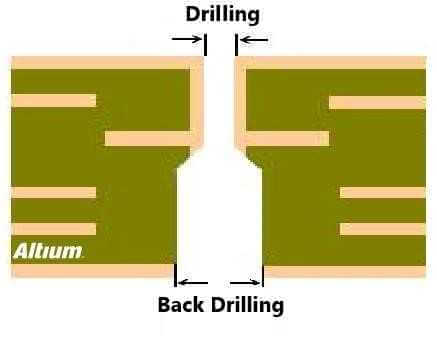
Back drill is actually a special drilling technique to control the depth of the hole. In the production of the multilayer board, such as the production of the 8-layer board, we need to connect the first layer to the sixth layer. The through-hole is usually drilled first (once) and then copper plated. So layer 1 goes directly to layer 8. In fact, we only need to connect the first layer to the sixth layer, and the seventh to the eighth layer, as there is no connection, is like an extra copper-plated column.
This column in high frequency and high-speed circuit design, will cause signal transmission reflection, scattering, delay and so on, to the signal integrity of the problem. So drill the extra column (STUB in the industry) from the back (second drill). Hence the name back drill.
Back drill is actually a special kind of deep control drill. In the production of multilayer board, for example, in the production of 12-layer board, we need to connect the first layer to the ninth layer. Usually, we drill through hole (one drill) and then make copper. In this way, the first floor is directly connected to the 12th floor. In fact, we only need the first floor to connect to the 9th floor. The 10th to the 12th floor is like a column because there are no lines to connect.
This column affects signal pathways and can cause signal integrity problems in communication signals. So drill the extra column (STUB in the industry) from the back (second drill). So called back drill, but generally not so clean, because the subsequent process will electrolyze away a bit of copper, and drill tip itself is also pointed. Therefore, PCB manufacturer will leave a little bit. The length of the STUB is called B value, which is generally in the range of 50-150um.
Besides design, material, transmission line, connector and chip package, the conduction hole has great influence on the signal integrity of signal system. The back drill eliminates the effect of extra stubs on signal integrity by drilling through holes without any connection or transmission. In addition, back drilling technology has the following advantages.
Reduce noise interference;
Improve signal integrity;
Local plate thickness becomes smaller;
Reduce the use of buried blind hole, reduce the difficulty of PCB production.
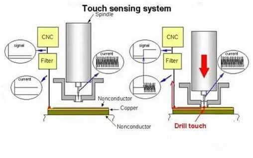
When drilling with the drilling needle, the micro current generated when the drilling needle tip contacts the copper foil on the substrate surface is used to sense the height of the board surface. Then, the drilling is carried out according to the set drilling depth, and the drilling is stopped when the drilling depth is reached.
The work diagram is shown as follows:
According to the PCB provided, the PCB shall be positioned by one drill and drilled by one drill. Deviation of one drill hole of back drill will increase the difference of alignment between back drill and one drill hole, which will have great influence on the accuracy of back drill, so the accuracy of one drill hole must be strictly controlled.
Electroplate a PCB after drilling. If there is not enough copper hole here, it will seriously affect the requirements. Need to use low current, long time, one-time enough plating. After electroplating, the thickness of copper is monitored by slicing. Electroplating parameters: 15ASF&Times;(48 min + 48 min).
Use the drill tool to drill the electroplated holes that need to be drilled back, two drill holes. Back drilling is to use the depth control function of the drilling machine to realize the blind hole processing to remove part of the hole copper. Its tolerance is mainly affected by the accuracy of backdrilling equipment and the tolerance of medium thickness.
Numerical plug hole for the whole hole. The back hole has a large end, a small end and a corner characteristic, theoretically more easy to produce bubble cavity, need to be effective plug hole.
The panel surface after the treatment of the plug hole is treated. Eliminate residue. Due to the great difference between copper surface and resin hardness, it is necessary to ensure the flat surface of the grinding plate.
The use of back drilling technology is unique. The requirements are complicated. It is commonly used in signal communication equipment, large servo, medical electronics, military, aerospace and other important fields. There are professional and deep technical reserves and research and development strength in this field, and high-end technology and product design are needed. In general, the back-drill PCB has the following technical characteristics.
Most backboards are hard
The number of floors is usually 8 to 50
Plate thickness: over 2.5mm
The thick diameter is larger
Large plate size
The outer circuit is less, and is mostly designed with square array of compression holes
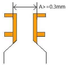
The minimum diameter of the first drill is generally greater than 0.3mm. The recommended bore size for a single drill shall be no less than 0.3mm. As shown in the figure below, the hole size of the first drill is denoted by A.
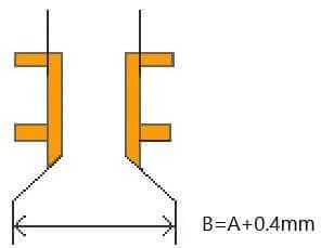
The back hole is usually 0.4mm larger than the hole to be drilled out. The hole diameter of back drilling is generally recommended to be 0.25mm~0.4mm larger than that of primary drilling. To be on the safe side, large 0.4mm is recommended. As shown in the figure below, the back-drilling aperture is represented by B.
Back drill depth control redundancy 0.2mm. The back drill is realized by using the depth control function of the drill. Since the drill tool of the back drill is pointed, there is always a small margin when drilling into the corresponding layer due to the inclination Angle of the drill tool. The back-drill depth control is recommended to retain at least 8mil or 0.2mm. Moreover, the thickness of the medium needs to be considered in the cascade setting to avoid the occurrence of wire breakage.
As shown in the figure below, back drill depth redundancy is represented by S.
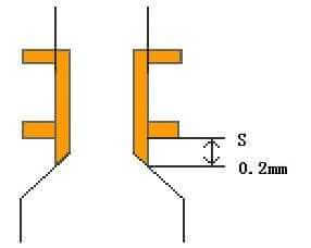
If the back drill requires drilling to M layer, the media thickness between adjacent undrilled layers with M layer is 0.3mm minimum.
Back drill and line spacing. The distance between the layer drop line by the stub of the back hole and the back hole is recommended to be no less than 10mil (0.25mm).
The back drilling technique and parameters to be considered in the design of back drilling are introduced. So in the Altium Designer, how to carry out the back drill design of each parameter setting? Use a specific case to show the Altium Designer in the back drill design method.
Step 1: Set up the drilling layer pairs
First punch holes and thread. For example, an 8-ply board, punch holes from the Top layer, and then switch to Midlayer1 to go up the wire. The remaining Midlayer2 to the bottom layer required Backdrilling. The first step here is to set up in the Design-Layer Stack Manager-Drill Pair. The bottom layer starts Midlayer2 and terminates the Bottom layer, as shown in the figure below. Be sure to check the Back Drill pair box to indicate that it is used for back drill holes
Step 2: Ensure that the interval between the signal layer Midlayer1 and the starting layer Midlayer2 of the back drill is no less than 0.3mm.
Step 3: Determine the length of the copper-plated column to be drilled from the back hole.
The Layer thickness from Midlayer2 to the bottom layer in the Layer Stack Manager adds up to about 1mm. he thickness of the layer between Midlayer1 and Midlayer2 on the stack manager page is exactly 0.254mm medium thickness due to the consideration of 8mil (0.2mm) redundancy of back drill control. therefore, the copper-plated column to be drilled can be set to about 1mm. of course, this value should be increased or decreased according to the specific design requirements of the engineer.
Step 4: Set Back-Drill size, depth, and network.
Set Max Stub Length and the depth of the copper-plated column to be drilled to 1 mm. et the size of the back hole to be 0.2mm larger than the radius of the original through hole. he diameter of the back hole and the original through hole is 0.4mm larger. Then set the through-hole network that needs back drilling to complete the rules setting of back drilling.
Note: PCB board factory’s back drill depth process capability needs to be communicated with the manufacturer.


XPCB Limited is a premium PCB & PCBA manufacturer based in China.
We specialize in multilayer flexible circuits, rigid-flex PCB, HDI PCB, and Rogers PCB.
Quick-turn PCB prototyping is our specialty. Demanding project is our advantage.
Tel : +86-136-3163-3671
Fax : +86-755-2301 2705
Email : [email protected]
© 2024 - XPCB Limited All Right Reserve
