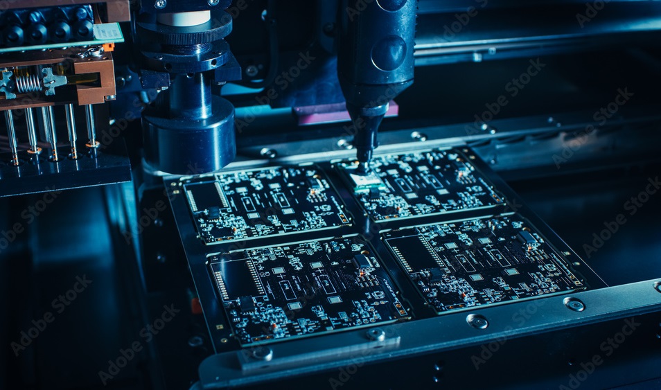
Component arrangement direction of reflow soldering process:
① The placement direction of the components should consider the direction of the printed circuit board entering the reflow oven.
②In order to make the two sides of the two-terminal chip components and the pins on both sides of the SMD component heat up synchronously, to reduce the tombstone, displacement, and the welding end from the welding due to the fact that the two sides of the components cannot be heated synchronously. Soldering defects such as disks require that the long axis of the two terminal chip components on the printed circuit board should be perpendicular to the direction of the conveyor belt of the reflow oven.
③ The long axis of the SMD components should be parallel to the transmission direction of the reflow oven, and the long axis of the chip components at the two ends and the long axis of the SMD components should be perpendicular to each other.
④ A good component layout design should not only consider the uniformity of heat capacity but also consider the arrangement direction and order of components.
⑤ For large-sized printed circuit boards, in order to keep the temperature on both sides of the printed circuit board as consistent as possible, the long side of the printed circuit board should be parallel to the direction of the conveyor belt of the reflow oven. Therefore, when the printed circuit board size is greater than 200mm, the requirements are as follows:
a) The long axes of the chip components at the two ends are perpendicular to the long sides of the printed circuit board.
b) The long axis of the SMD component is parallel to the long side of the printed circuit board.
c) A printed circuit board assembled on both sides, with the same orientation of components on both sides.
d) The arrangement direction of components on the printed circuit board. Similar components are arranged in the same direction as much as possible, and the characteristic directions should be consistent, which is convenient for component mounting, welding and testing. For example, the positive electrode of the electrolytic capacitor, the positive electrode of the diode, the single-pin end of the triode, and the first pin of the integrated circuit are arranged in the same direction as possible.
In order to prevent short circuit between layers caused by touching the printed wires during PCB processing, the distance between the conductive patterns on the edge of the inner layer and the outer layer should be greater than 1.25mm from the edge of the PCB. When the edge of the outer layer of the PCB has been routed with the ground line, the ground line can occupy the edge position. For the position of the PCB board that has been occupied due to structural requirements, components and printed wires cannot be laid out. There can be no through holes in the bottom pad area of the SMD/SMC to avoid the solder being heated and remelted in the wave soldering after reflow soldering shunt.
Installation spacing of components:
The minimum installation spacing of components must meet the requirements of manufacturability, testability and maintainability of SMT chip processing.


XPCB Limited is a premium PCB & PCBA manufacturer based in China.
We specialize in multilayer flexible circuits, rigid-flex PCB, HDI PCB, and Rogers PCB.
Quick-turn PCB prototyping is our specialty. Demanding project is our advantage.
Tel : +86-136-3163-3671
Fax : +86-755-2301 2705
Email : info@x-pcb.com
© 2024 - XPCB Limited All Right Reserve