- +86-755-23012705
- Building 3, Jinfeng Industrial Park, Fuyong Street, Baoan District, Shenzhen ,China
- [email protected]
HDI (High Density Interconnect) technology allows for a denser design on the PCB and thus potentially smaller PCBs with more traces and/or components in a given area. As a result, the paths between components can be shorter. HDIs use blind/buried vias, or a combination that includes microvias. With multi-layer HDI PCBs the interconnection of several vias stacked on top of each other (stacked vías, instead of one deep buried via) can be made stronger, thus enhancing reliability in all conditions.
Since the printed circuit board is not a general end product, the definition of the name is slightly confusing, for example, the motherboard for personal computers is called a motherboard and cannot be directly called a circuit board, although the existence of a circuit board in the motherboard is not the same. So the two are related but cannot be said to be the same when evaluating the industry. Another example: because there are integrated circuit parts loaded on the circuit board, the news media call it an IC board, but in essence, it is not the same as a printed circuit board.
Under the premise that electronic products tend to be multi-functional and complex, the contact distance of integrated circuit components is reduced, the speed of signal transmission is relatively increased, and the number of wiring is increased, and the length of wiring between points is shortened locally, which requires the application of HDI(high density Interconnect) circuit board configuration and microvia technology to achieve the goal.

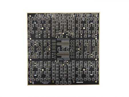
Image 1: 8L HDI PCB prototype by XPCB Limited
Wiring and jumper are basically difficult to achieve for single and double panels, so the circuit board will move towards multi-layer, and due to the continuous increase of signal lines, more power planes and ground planes are necessary means of design, which makes multilayer printed circuit boards more common.
In order to electrically require high-speed signals, the circuit board must provide impedance control with alternating current characteristics, high-frequency transmission capability, and reduction of unwanted radiation (EMI). With the structure of stripline and microstrip, multi-layering is necessary. In order to reduce the quality of signal transmission, insulating materials with low dielectric coefficient and low attenuation rate are used, and the density of the circuit board is continuously increased to meet the needs of miniaturization and array of electronic components.
The emergence of BGA (Ball Grid Array), CSP (Chip Scale Package), DCA (Direct Chip Attachment) and other component assembly methods has pushed printed circuit boards to an unprecedented high-density realm. Holes with a diameter of less than 150um are called microvia in the industry, and circuits made by using the geometric structure technology of this microvia can improve the efficiency of assembly, space utilization, etc., and at the same time, it is necessary for the miniaturization of electronic products.

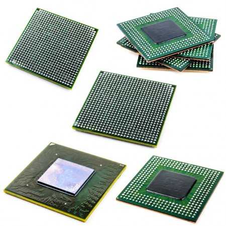
Image 2: BGA products of HDI
There have been many different names for circuit boards with this type of structure. For example, European and American companies used to call this type of product SBU (Sequence Build Up Process) because the program they produced was a sequential construction method, which is generally translated as “sequential layer addition method”.
As for Japanese manufacturers, the hole structure of these products is much smaller than that of conventional products, so the manufacturing technology of this type of product is called MVP (Micro Via Process), which is generally translated as “Micro Via Process”. There are also people who call this type of board BUM (Build Up Multilayer Board) because the traditional multilayer board is called MLB (Multilayer Board), which is generally translated as “multilayer board”.
In order to avoid confusion, the IPC Board Association of the United States proposed to call this type of product HDI (High Density Intrerconnection Technology) a generic name, and if it is directly translated, it becomes a high-density connection technology. However, this does not reflect the characteristics of the circuit board, so most circuit board manufacturers call this type of product HDI board or the full Chinese name “high-density interconnection technology”. However, because of the problem of speaking fluency, some people directly call this type of product “high-density circuit board” or HDI board.

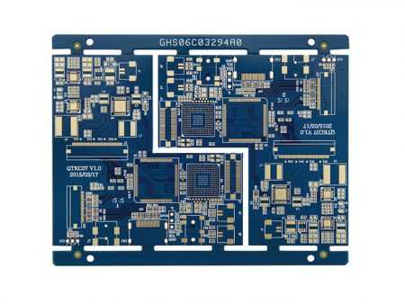
Image 3: HDI Rigid PCB
Take Your Projects to New Heights with XPCB Limited
XPCB Limited offers top-notch PCB manufacturing, quick-turnaround prototyping, and turnkey PCBA services designed to make your projects shine. Count on us to bring your ideas to life with efficiency and quality. Your success matters to us, and we’re here to make your innovation journey smooth and rewarding.


XPCB Limited is a premium PCB & PCBA manufacturer based in China.
We specialize in multilayer flexible circuits, rigid-flex PCB, HDI PCB, and Rogers PCB.
Quick-turn PCB prototyping is our specialty. Demanding project is our advantage.
Tel : +86-136-3163-3671
Fax : +86-755-2301 2705
Email : [email protected]
© 2024 - XPCB Limited All Right Reserve
