- +86-755-23012705
- Building 3, Jinfeng Industrial Park, Fuyong Street, Baoan District, Shenzhen ,China
- [email protected]
Menu
Definition of printed circuit board
Printed circuit boards (PCBS) appear in almost every electronic device. If there are electronic components in a device, they are all mounted on PCBS of different sizes. In addition to fixing various small parts, PCB’s main function is to provide electrical connections between the above parts. As electronic devices become more complex and require more parts, PCB’s become denser in wiring and parts.
A standard PCB with no components on the board, PCB often referred to as “Printed Wiring Board (PWB).”
The substrate of Rigid PCB is made of an insulating, heat-insulating material that is not easily bent. The small wiring material that can be seen on the surface is copper foil. Originally, copper foil covers the whole board, but in the manufacturing process, the middle part is etched away and the remaining part becomes a network of small wiring.
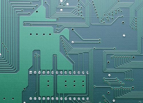
These lines are called the conductor pattern, or wiring, and are used to provide electrical connections for parts on a PCB. To fix the parts to the PCB, we weld their pins directly to the wiring.
On the most basic PCB (single side), the parts are concentrated on one side and the wires on the other. In this way, we need to make holes in the board so that the connector can pass through the board to the other side, so the connector of the part is welded to the other side. On account of this, the sides of a PCB are called Component Side and Solder Side, respectively.
If there are some parts on the PCB that need to be removed or put back after production, the part will be installed with a Socket. As the socket is directly welded to the board, the parts can be arbitrarily disassembled.
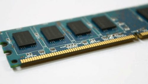
To connect two PCBS, we usually use the edge Connector, commonly known as the “goldfinger”. Goldfinger contains many exposed copper pads that are actually part of the PCB layout. Usually when connected, we insert the golden finger on one PCB into the appropriate Slot on the other PCB (commonly called expansion Slot). In computers, graphics, sound, and similar interface CARDS are connected to the motherboard by the goldfinger.
The green or brown color on a PCB is the color of solder mask. This is an insulating layer that protects the copper wire and prevents parts from being welded in the wrong place. On the welding barrier layer, another silk screen will be printed. Words and symbols (mostly white) are often printed to indicate where the parts are on the board. The screen-printing surface is also known as Legend.
The printed circuit board etches the copper wire of the complex circuit between parts on a board after careful and neat planning. It provides the main support body for the installation and interconnection of electronic components. It is an indispensable basic part of all electronic products.
Printed circuit board a flat plate made of nonconductive material on which preboard holes are usually designed for the installation of chips and other electronic components. The holes in the assembly help to electronically connect the metal paths that are pre-defined and printed on the board, passing the connector pins through the PCB, and then attaching the conductive metal electrode to the PCB to form a circuit.
According to its application field, PCB can be divided into single panel, double panel, multi-layer board and soft board with more than four layers. Generally speaking, the more complex the functions of electronic products, the longer the loop distance and the more the number of contact feet, the more layers are required for PCB, such as high-end consumer electronics, information and communication products. FPC is mainly used in products that need to be wound: such as notebook computers, cameras, automobile instruments, etc.
The principle of printed circuit board
The working principle of the circuit board is to use the board base insulation material to separate the surface copper foil conductive layer, so that the current flow along the pre-designed route in various components to complete functions such as work, amplification, attenuation, modulation, demodulation, coding and so on.
On the most basic PCB (single side board), the parts are concentrated on one side and the wires on the other. Because the wires only appear on one side, the PCB is called a single panel.
Layers of wires must be properly connected between the two layers. The bridge between the two circuits is called a guide hole (VIA).
The basic design process of circuit board can be divided into the following four steps:
(1) Design of circuit schematic diagram — The design of circuit schematic diagram mainly USES Protel DXP schematic editor to draw the schematic diagram.
(2) Generate reports – network statement that shows the links of all components in the circuit principle and relationship of the report, it is connected to circuit schematic design and circuit board design of bridge and link, through the network statements circuit schematic diagram, can quickly find the components, the relation between which provide convenience for the back of the PCB design.
(3) Design of printed circuit board — the design of printed circuit board is commonly referred to as PCB design, which is the final form of circuit schematic diagram. Related design of this part is more difficult than the design of circuit schematic diagram. We can complete this part of design with the help of the powerful design function of Protel DXP.
(4) Generate PRINTED circuit board report — After the design of printed circuit board is completed, it is necessary to generate various reports, such as generate pin report, circuit board information report, network status report, etc., and finally print out the printed circuit diagram.
Rigid PCB is mainly composed of welding plate, through hole, installation hole, wire, components, connectors, filler, electrical boundary and so on. Common board structures include Single Layer PCB, Double Layer PCB and Multi-Layer PCB.
The main functions of each component are as follows:
Solder pad: Metal hole used for welding pins of components.
Through hole: There are through hole (PTH) and non through hole, in which the through-hole is used to connect the component pins between each layer.
Mounting hole: used for fixing circuit board.
Conductor: Electrical network copper film used to connect the pins of components.
Connectors: Components used to connect circuit boards.
Filling: Copper coating used in ground wire networks to effectively reduce impedance.
Electrical boundary: Used to determine the size of the circuit board, all components on the circuit board should not exceed this boundary.
PCB can be divided into rigid PCB and flexible PCB according to the production materials. Rigid circuit board is mainly made of copper-clad plate (CCL) as the base material. The rigid printed boards are phenolic paper laminate, epoxy paper laminate, polyester glass felt laminate, epoxy glass cloth laminate.
Manufacture of printed circuit boards
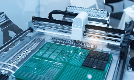
Printed circuit board (PCB) is a structural component formed by insulating material and conductor wiring. When the final product is made, integrated circuits, transistors, diodes, passive components (such as resistors, capacitors, connectors, etc.) and various other electronic components are installed. Through wire connection, electronic signals can be formed to connect and function. The PRINTED circuit board (PCB) is therefore a platform that provides component connections and serves as the basis for connecting components.
Because printed circuit boards are not general end products, the definition of the name is somewhat confusing. For example, the motherboard used in personal computers is called the motherboard, but not directly called the circuit board. Although there are circuit boards in the motherboard, but not the same, so the two are related but not the same when evaluating the industry.
Another example: the news media calls it an IC board because an integrated circuit component is mounted on a circuit board, but it is not essentially the same as a printed circuit board.
Under the preconditions that electronic products tend to be multi-functional and complicated, the contact distance of integrated circuit components will be reduced and the speed of signal transmission will be relatively increased, followed by the increase in the number of connections and the local shortening of the length of wiring between points, which requires the application of high-density line configuration and micro-hole technology to achieve the goal.
Wiring and bonding are basically difficult for single and double panels, so the Circuit Board will be multilayered. Moreover, due to the continuous increase of signal lines, more power layers and connection layers are the necessary means of design. All these make multi-layer Printed Circuit Board more common.
For high speed signal electrical requirements, the circuit board must provide impedance control with alternating current characteristics, high frequency transmission capacity, reduce unnecessary radiation (EMI), etc. With Stripline and Microstrip structure, multilayer becomes a necessary design.
In order to reduce the quality problem of signal transmission, insulating materials with low dielectric coefficient and attenuation rate will be adopted. In order to match the miniaturization and array of electronic components, the density of circuit boards will be increased continuously to meet the demand. BGA (Ball Grid Array), CSP (Chip Scale Package), DCA (Direct Chip Attachment) and other parts assembly methods promote printed circuit boards to unprecedented high density.
Any hole with a diameter less than 150um is called Microvia in the industry. The circuit made by using the geometric structure technology of microholes can improve the efficiency of assembly, space utilization and so on. Meanwhile, it is also necessary for the miniaturization of electronic products.
For this kind of structure of the circuit board products, the industry has had a number of different names to call such a circuit board. For example, European and American companies used to Sequence Build Up Process for their programs, so they called such products SBU (sequential Build Up Process).
As for the Japanese manufacturers, because the hole structure of such products is much smaller than that of the previous ones, they call the manufacturing technology of such products MVP (Micro Via Process), which is generally translated as “Micro Via Process”.
Some people also call such circuit boards BUM (Build Up multi-layer Board) because the traditional multi-layer boards are called MLB (multi-layer Board), which is generally translated as “multi-layer Board”.
High density: For more than 100 years, PCB high density has been developing with the improvement of integrated circuit integration and installation technology.
High reliability: through a series of inspection, testing and aging tests, PCB can be guaranteed to work reliably for a long term (service life, generally 20 years).
Designability: PCB’s various properties (electrical, physical, chemical, mechanical, etc.) can be designed through design standardization, standardization and so on to achieve the printed board design, short time, high efficiency.
Producibility: with modern management, standardization, scale (quantity), automation and other production can be carried out to ensure the consistency of product quality.
Testability: complete test methods, test standards, various test equipment and instruments have been established to test and identify PCB product conformity and service life.
Electronic equipment with printed board, because of the consistency of the same kind of printed board, so as to avoid the error of manual wiring, and can realize the electronic components automatically insert or paste, automatic soldering, automatic detection, to ensure the quality of electronic equipment, improve labor productivity, reduce the cost, and easy to maintain.
Consumer electronics: This includes all the electronics we use in our lives. From audio and video systems, televisions, video and DVD players, digital cameras, computers and laptops, mobile phones and GPS to home and kitchen appliances. These devices often use standard PCBS that are fairly standard and similar to each other.
Medical devices: HIGH density PCB can be used in medical devices. They support the use of more intensive designs to test new and advanced medical technologies. It also reduces the complexity of making small, lightweight medical devices. PCBs are suitable for medical devices of all sizes, from small pacemakers to large X-ray and CAT machines.
Industrial machinery: PCBs are commonly used in high-power industrial machinery. Thick copper PCBs are commonly found in industrial machinery to better meet important requirements.
For example, heavy copper PCBS can be found in industrial machines such as motor controllers, industrial load testers and high-current battery charging.
LED applications: LED lights are another common TYPE of PCB device, a more modern form of technology, but still largely based on PCBs, which are known for increasing power consumption.
LED lamps have PCBs that act as radiators, allowing higher levels of heat transfer than ordinary PCBs. Even some other basic lighting solutions use these aluminum backplanes for high level heat transfer.
Automotive and aerospace related equipment: PCB is designed to withstand high vibration environment and can be used in automotive and aerospace industry related equipment. Flexible PCB supports vibration characteristics of these industries. They can be very flexible and can be adapted to very small Spaces designed within the device. PCB’s in these devices can also be very lightweight and durable, which is critical for manufacturing transportation components and for industries with high impact, low weight requirements.
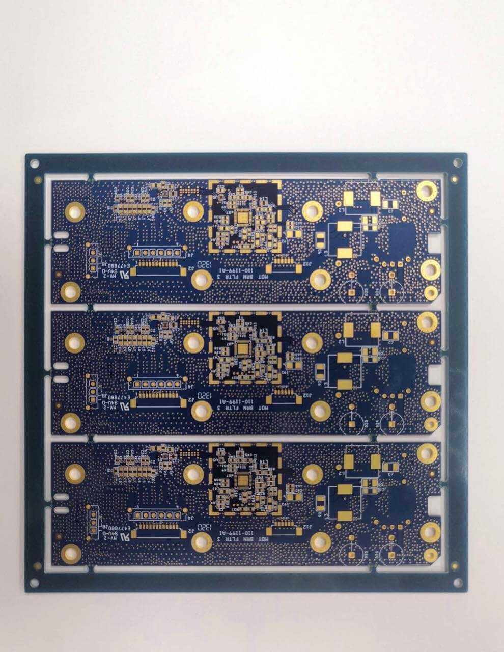
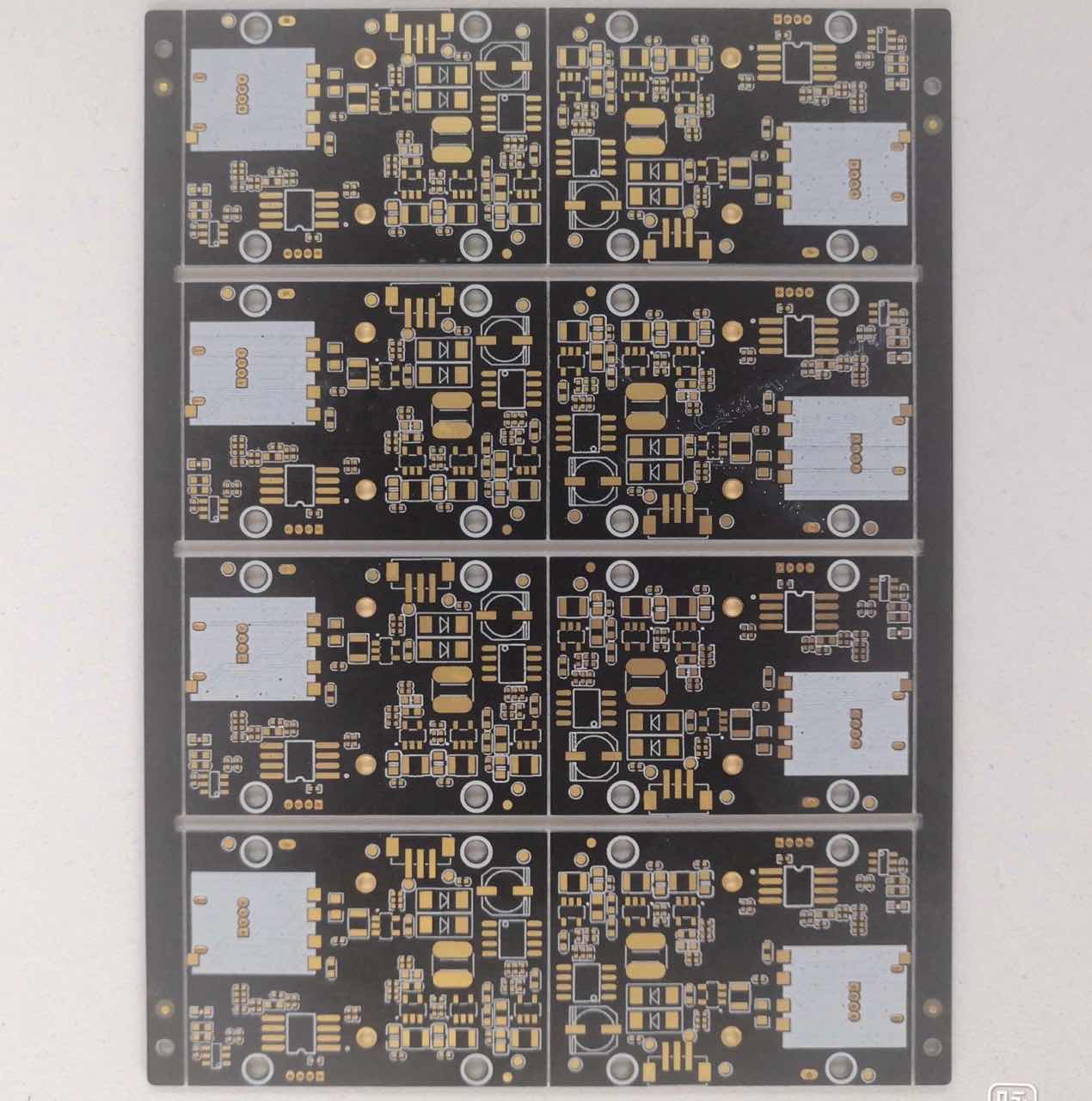
XPCB not only produces Rigid PCB, but also devotes itself to the manufacturing of more detailed and complicated PCB for more than ten years.


XPCB Limited is a premium PCB & PCBA manufacturer based in China.
We specialize in multilayer flexible circuits, rigid-flex PCB, HDI PCB, and Rogers PCB.
Quick-turn PCB prototyping is our specialty. Demanding project is our advantage.
Tel : +86-136-3163-3671
Fax : +86-755-2301 2705
Email : [email protected]
© 2023 - XPCB Limited All Right Reserve
