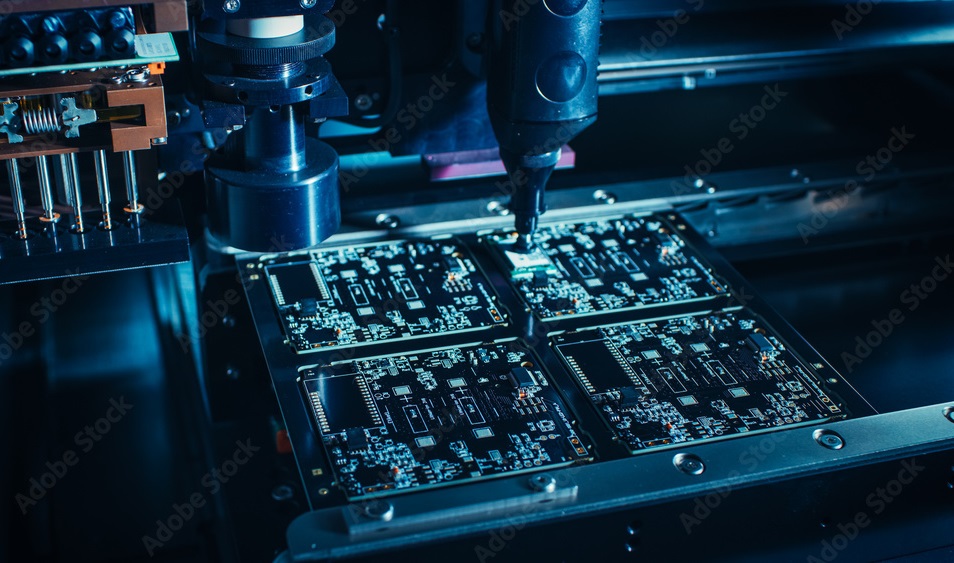


The exact position of the BGA component on the circuit board depends entirely on the accuracy of the chip placement machine. Most of the placement machines include a specific positioning system that can help achieve the precise positioning of the BGA component. In addition, some chip mounters can even check the coplanarity of BGA solder balls and identify some defects, such as missing solder balls, which is very helpful for improving the reliability of BGA soldering.
In addition, some other measures can be taken to further improve the installation accuracy of BGA components. For example, a local fiducial mark is set on the outside of the BGA pad, or several fold lines are set as fiducial marks for manual inspection after assembly. Both methods have been verified in actual manufacturing.
Due to the surface tension of the solder, BGA components have obvious self-centering effects during the soldering process. Therefore, some designers deliberately add pads on the four corners in the BGA pad design to make the self-centering effect more obvious. To ensure that the BGA components can be automatically reset after shifting the installation position.
The welding temperature profile directly determines the welding quality. The temperature curve usually includes four stages: preheating stage, soaking stage, reflux stage and cooling stage. Each stage has different physical/chemical changes. Since the setting of the temperature curve determines the formation process of the solder joint, it is closely related to the reliability of the solder joint. Due to the particularity of the BGA package, it is very difficult to generate a satisfactory temperature profile. Generally speaking, BGA components need to measure three temperatures: package temperature, circuit board surface temperature and internal solder joint temperature of BGA.
Since all BGA solder joints are under the package after soldering, traditional inspection methods (such as flying probe test or visual inspection) cannot meet actual needs. So far, the leading methods that can scan BGA solder joints for welding defects are AOI (Automatic Optical Inspection) testing and AXI (Automatic X-ray Inspection) testing.
According to the characteristics of the BGA structure, it is almost impossible to inspect a single solder joint of a BGA component. However, the entire package should be repackaged.
Other factors must be paid attention to during the BGA assembly process, such as electrostatic protection and BGA component baking. Generally, BGA components require special packages with electrostatic protection requirements. During the assembly process of printed circuit boards, strict electrostatic protection measures should be taken, including equipment grounding, personnel management and environmental management.
XPCB Limited is a premium PCB & PCBA manufacturer based in China.
We specialize in multilayer flexible circuits, rigid-flex PCB, HDI PCB, and Rogers PCB.
Quick-turn PCB prototyping is our specialty. Demanding project is our advantage.
Tel : +86-136-3163-3671
Fax : +86-755-2301 2705
Email : [email protected]
© 2024 - XPCB Limited All Right Reserve
