- +86-755-23012705
- Building 3, Jinfeng Industrial Park, Fuyong Street, Baoan District, Shenzhen ,China
- [email protected]
HDI PCBs (High-density interconnect PCB) represent one of the fastest-growing segments of the printed circuit board market. Due to the higher circuit density of HDI PCBs, it is possible to incorporate thinner lines and spaces, smaller through-hole and capture pads, and higher connection pad densities when designing. HDI PCBs have both blind and buried vias and typically contain microvias with a diameter of 0.006 or less. So, what are the main applications of HDI PCB circuit boards?
Blind Via Hole: The outermost circuit of the blind buried via circuit board is connected with the adjacent inner layer with plating holes, which is called “blind pass” because the opposite side cannot be seen. To increase the space utilization of the PCB circuit layer, the “blind via” process came into being. This production method needs to pay special attention to the depth of the drilling hole (Z-axis) to be just right, this method often causes the difficulty of electroplating in the hole, so it is almost adopted by no manufacturer;
Blind vias are located on the top and bottom surfaces of the printed circuit board and have a certain depth and are used for the connection of the surface line and the inner layer line below, and the depth of the hole usually does not exceed a certain ratio (hole diameter).
In non-penetrating via technology, the application of blind and buried vias can greatly reduce the size and quality of blind and buried hole circuit boards, reduce the number of layers, improve electromagnetic compatibility, increase the characteristics of electronic products, reduce costs, and make the design work easier and faster. In traditional PCB design and fabrication, through-holes present a number of problems.
First of all, they occupy a large amount of effective space, and secondly, a large number of through-holes are concentrated in one place, which also causes a huge obstacle to the inner layer of the multi-layer PCB, these through-holes occupy the space required for the traces, they densely pass through the surface of the power supply and ground layer, and also destroy the impedance characteristics of the power ground layer, so that the power ground layer fails. And conventional mechanical drilling will be 20 times the workload of using non-penetrating pilot hole technology.

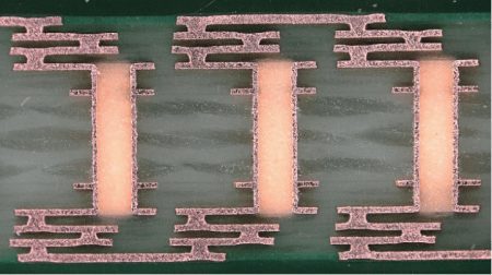
HDI stackup
In PCB design, although the size of pads and vias has gradually decreased, if the thickness of the board layer does not decrease proportionally, the aspect ratio of the through hole will increase, and the aspect ratio of the through hole will increase, and the aspect ratio of the through hole will reduce the reliability. With the maturity of advanced laser drilling technology and plasma dry corrosion technology, it is possible to apply non-penetrating small blind holes and small buried holes, if the diameter of these non-penetrating holes is 0.3mm, the parasitic parameters brought by it are about 1/10 of the original conventional holes, which improves the reliability of the PCB.
Due to the non-penetrating via technology, there are fewer large vias on the CBVIA board, which provides more space for traces. The remaining space can be used for large-area shielding to improve EMI/RFI performance. At the same time, more free space can be used for the inner layer to partially shield the device and critical network cables for optimal electrical performance. The use of non-pilot vias makes it easier to fan out the device pins, making it easy to route high-density leaded devices, such as BGA package devices, to shorten the wire length and meet the timing requirements of high-speed circuits.
The development of HDI PCB technology has given engineers unprecedented design freedom and flexibility to place more components on both sides of the original PCB as needed, while allowing smaller components to be placed together. This means that HDI PCBs ultimately lead to faster signal transmission as well as enhanced signal quality.
HDI PCBs are widely used to reduce the weight and overall size of products, as well as to enhance the electrical performance of devices, and are often found in mobile phones, touchscreen devices, laptops, digital cameras, and 4G network communications. HDI PCBs are also prominent in medical devices as well as various electronic aircraft components.

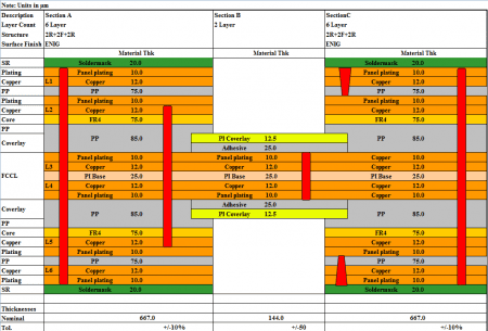
6 layer HDI rigid flex pcb stackup
HDI PCBs are suitable for a variety of industries. As mentioned above, you will find them in all types of digital devices such as smartphones and tablets, and miniaturization is the key to the effective application of the product. You can also find it in cars, planes, and other vehicles that rely on electronics.
One of the most critical areas where high-density PCBs have made great progress is in the medical field. Medical devices often require small packages with high transfer rates, which only HDI PCBs can provide. For example, the implant needs to be small enough to fit the human body, but any electronic devices involved in the implant absolutely must effectively allow for high-speed signal transmission. In addition, other medical devices such as emergency room monitors, CT scans, etc. are also available on HDI PCBs.
Take Your Projects to New Heights with XPCB Limited
XPCB Limited offers top-notch PCB manufacturing, quick-turnaround prototyping, and turnkey PCBA services designed to make your projects shine. Count on us to bring your ideas to life with efficiency and quality. Your success matters to us, and we’re here to make your innovation journey smooth and rewarding.


XPCB Limited is a premium PCB & PCBA manufacturer based in China.
We specialize in multilayer flexible circuits, rigid-flex PCB, HDI PCB, and Rogers PCB.
Quick-turn PCB prototyping is our specialty. Demanding project is our advantage.
Tel : +86-136-3163-3671
Fax : +86-755-2301 2705
Email : [email protected]
© 2024 - XPCB Limited All Right Reserve
