- +86-755-23012705
- Building 3, Jinfeng Industrial Park, Fuyong Street, Baoan District, Shenzhen ,China
- [email protected]
In the fast-paced world of electronics, the demand for smaller, faster, and more reliable devices continues to drive innovation. One of the key technologies enabling this revolution is High-Density Interconnect (HDI) PCB technology. HDI PCBs are rapidly transforming industries, from consumer electronics to automotive, medical devices, and telecommunications. By offering high-density circuits in smaller spaces, HDI PCBs are not only meeting the needs of modern devices but are also paving the way for more sophisticated and efficient electronics. In this blog, we’ll explore how HDI PCB technology is changing the landscape of electronics and why it has become a critical component in advanced product designs.
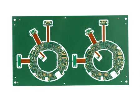
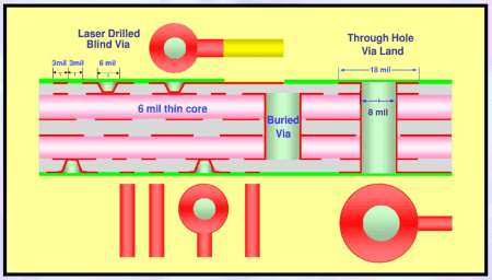
HDI (High-Density Interconnect) PCB is a type of printed circuit board that features finer traces, smaller vias, and more compact layer configurations compared to traditional PCBs. HDI technology allows for a greater density of components and interconnections in a smaller area, which leads to improved performance and reliability. This is achieved through advanced manufacturing techniques, such as microvias, laser-drilled vias, blind and buried vias, and fine-pitch components, which are not typically used in standard PCB designs.
The key difference between an HDI PCB and a traditional PCB lies in the density and complexity of the interconnections. While traditional PCBs are often limited by the number of layers and the size of the traces, HDI PCBs utilize smaller components and more intricate designs to achieve higher functionality in a compact footprint.

HDI PCBs are playing a transformative role in a variety of modern electronic applications. Here are some ways they are revolutionizing the industry:
One of the most significant advantages of HDI PCBs is their ability to support miniaturization. As consumer electronics such as smartphones, tablets, and wearables become smaller, the demand for PCBs that can pack more functionality into a limited space has grown. HDI technology allows for smaller vias, thinner layers, and higher component density, enabling designers to create smaller devices without compromising on performance. This is particularly important in industries where space is at a premium, such as in wearable devices or Internet of Things (IoT) products.
HDI PCBs improve the overall signal integrity and data transfer speeds by reducing the distance signals must travel between components. The microvias used in HDI PCBs reduce the need for long trace paths, which can introduce signal delays and noise in high-speed circuits. The shorter, more direct paths of HDI PCBs contribute to faster, more reliable signal transmission, which is crucial in applications such as 5G communication, high-frequency electronics, and advanced computing.
For instance, 5G networks rely heavily on HDI PCBs to support the high-density interconnections needed for transmitting large volumes of data at faster speeds. As the need for faster wireless communication and higher processing power grows, HDI PCBs play an essential role in enabling these technologies.
In the world of electronics, especially in mission-critical applications such as aerospace, automotive, and medical devices, reliability is paramount. HDI PCBs offer superior performance under harsh conditions, such as high temperatures, vibrations, and mechanical stresses, compared to traditional PCBs. The compact nature of HDI PCBs reduces the chances of component failure, making them ideal for demanding environments where durability is essential.
For example, in automotive electronics, HDI PCBs are used to support critical systems like advanced driver assistance systems (ADAS), infotainment systems, and electric vehicle (EV) control units. These systems must operate reliably in challenging conditions, including high heat, vibrations, and exposure to environmental factors, all of which are effectively handled by HDI technology.
Although HDI PCBs can be more expensive to manufacture initially due to the advanced technology and processes involved, they can be cost-efficient in high-volume production. The ability to pack more functionality into a smaller footprint can result in reduced material costs, fewer components, and simpler designs. For example, the integration of more functions on a single HDI board can reduce the need for additional connectors, cables, and circuit boards, ultimately lowering the overall manufacturing cost.
Moreover, the smaller size of HDI PCBs means that devices are lighter and more compact, which can reduce shipping and handling costs. In industries like consumer electronics, where companies rely on economies of scale, HDI PCBs can help manufacturers meet market demands more efficiently while maintaining competitive pricing.

HDI PCBs are enabling the development and advancement of several emerging technologies, including:
Autonomous Vehicles: HDI PCBs are used in various automotive systems, such as radar, cameras, and sensors, essential for autonomous driving. These systems require high-density interconnections and miniaturization to operate effectively within the limited space available in modern vehicles.
Medical Devices: From wearable health monitors to implantable devices, HDI PCBs are playing a key role in the development of advanced medical electronics. These devices need to be compact, reliable, and capable of supporting high-speed data transmission, all of which are enabled by HDI technology.
Smartphones and Wearables: As smartphones become more sophisticated, with features such as facial recognition, augmented reality (AR), and wireless charging, HDI PCBs are crucial in supporting the increasing complexity and miniaturization of these devices.
The future of HDI PCB technology looks promising, with innovations on the horizon that will further enhance its capabilities. These include:
Advanced materials: The development of new materials with higher thermal conductivity and electrical performance will enable HDI PCBs to support even faster speeds and higher frequencies.
3D stacking: Techniques like 3D stacking will allow for even greater component density and integration on a single board, which will be crucial in the development of next-generation electronics.
5G and beyond: As 5G technology becomes more widespread, the need for high-performance, high-density PCBs will continue to grow, driving further advancements in HDI PCB manufacturing.

HDI PCB technology is revolutionizing the way modern electronics are designed and manufactured. By enabling miniaturization, improved performance, increased reliability, and cost efficiency, HDI PCBs are helping to meet the demands of the most advanced technologies in industries such as telecommunications, automotive, consumer electronics, and medical devices. As devices continue to get smaller, faster, and more complex, HDI PCBs will remain at the forefront of innovation, driving the future of electronics.
Discover a World of Possibilities with XPCB Limited
At XPCB Limited, we’re here to help you explore new horizons. Our advanced PCB manufacturing, rapid prototyping, and turnkey PCBA solutions make it easy for you to turn your ideas into reality. Trust us to deliver excellence and reliability every step of the way. Join us and experience the power of innovation with XPCB Limited by your side.


XPCB Limited is a premium PCB & PCBA manufacturer based in China.
We specialize in multilayer flexible circuits, rigid-flex PCB, HDI PCB, and Rogers PCB.
Quick-turn PCB prototyping is our specialty. Demanding project is our advantage.
Tel : +86-136-3163-3671
Fax : +86-755-2301 2705
Email : [email protected]
© 2024 - XPCB Limited All Right Reserve
