- +86-755-23012705
- Building 3, Jinfeng Industrial Park, Fuyong Street, Baoan District, Shenzhen ,China
- [email protected]
In today’s fast-paced world, the demand for smaller, faster, and more powerful electronic devices has never been greater. From smartphones and wearables to medical devices and automotive systems, modern electronics require compact designs without compromising performance. High-Density Interconnect (HDI) technology has emerged as a key enabler in meeting these demands. By using advanced manufacturing techniques, HDI technology allows for high-performance circuit boards that are also smaller and more efficient. In this blog, we will explore how HDI technology addresses the needs of miniaturization and high performance in modern electronics.
HDI (High-Density Interconnect) technology refers to the use of advanced techniques to create printed circuit boards (PCBs) with higher component density and improved performance compared to traditional PCBs. This is achieved through the use of microvias, fine-pitch components, and multiple layers that allow for more efficient use of space. The primary goal of HDI technology is to enable the creation of smaller, more complex, and more reliable PCBs, which is crucial for modern electronics that demand both high functionality and compact size.

One of the key features of HDI technology is the use of microvias. Microvias are small, high-precision holes drilled into the PCB to connect layers. Unlike traditional vias, which are larger and require more space, microvias allow for dense interconnections in much smaller areas. This is a critical component in enabling the miniaturization of electronic devices.
Laser-Drilled Microvias: Microvias are typically created using laser drilling technology, which allows for extremely fine and accurate vias with diameters as small as 50 microns. The ability to create such tiny interconnections enables the board to be more compact, with fewer layers and less material, thus reducing the overall size of the PCB without sacrificing performance.
Stacked Microvias: HDI PCBs often use stacked microvias, which connect multiple layers of the PCB. This reduces the need for traditional through-hole vias, which take up more space and require more manufacturing steps. Stacked microvias enable the routing of signals and power in a 3D space, allowing for even higher density and miniaturization.
By incorporating microvias, HDI technology significantly reduces the space required for interconnections, allowing for more components to fit in a smaller area. This is especially important in applications like smartphones, wearables, and medical devices, where small size and lightweight are essential.
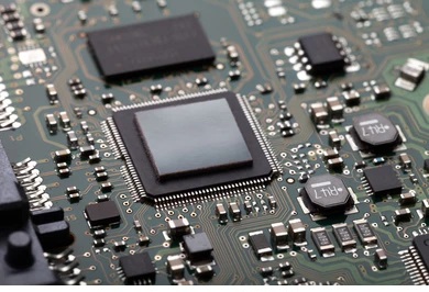
As electronic devices become more powerful, they require more components to handle complex functions. HDI technology allows for the use of fine-pitch components, which have smaller lead pitches, or the distance between leads. Fine-pitch components, such as Ball Grid Arrays (BGAs), Chip-on-Board (COB) packages, and Surface-Mount Technology (SMT) components, can be placed closer together, improving component density and performance.
Improved Signal Integrity: HDI PCBs provide superior signal integrity compared to traditional PCBs. The shorter trace lengths, enabled by fine-pitch components, result in faster signal transmission with reduced delays and attenuation. This is particularly important in high-speed applications like telecommunications, networking, and high-definition video processing, where signal quality is crucial.
Higher Frequency Support: Fine-pitch components and HDI design principles are also ideal for high-frequency circuits. In applications like wireless communication, radio frequency (RF) systems, and radar technologies, HDI PCBs can handle the higher frequency signals without degradation, ensuring high performance in compact form factors.
By allowing for more components to be placed within a smaller area and reducing the distance between them, HDI technology helps to achieve the higher performance required by modern electronics. These fine-pitch components are crucial for meeting the increasing complexity of electronic devices while maintaining speed and reliability.
Another important aspect of HDI technology is the use of multiple layers in PCB design. Traditional PCBs are typically limited to two or four layers, but HDI PCBs can incorporate 6, 8, or even more layers, depending on the design requirements. These additional layers allow for more routing space for signals and power, without increasing the overall size of the board.
Layer Stacking: By stacking multiple layers within a single PCB, HDI technology allows for more complex routing and higher component density without expanding the board’s footprint. This enables the design of more intricate circuits with greater functionality, while maintaining a small and compact size.
Power Distribution: The additional layers in HDI PCBs also allow for improved power distribution. By creating dedicated layers for power and ground planes, HDI technology ensures that the power supply to components is stable and consistent, which is essential for high-performance applications that require reliable power delivery.
The ability to integrate multiple layers into a single PCB without increasing the size is crucial for high-end applications, where space is limited but performance demands are high.

In high-performance devices, managing heat is critical to ensuring long-term reliability and optimal performance. HDI technology offers better thermal management capabilities than traditional PCBs, which is particularly important for miniaturized devices that contain more components in less space.
Thermal Vias: HDI PCBs often incorporate thermal vias—vias that are specifically designed to conduct heat away from high-power components. These thermal vias are strategically placed around heat-sensitive components to dissipate heat more efficiently and prevent overheating, which can damage sensitive electronics.
Advanced Materials: HDI PCBs often use advanced materials that have better thermal conductivity, such as ceramics or high-performance epoxy resins. These materials help to reduce the thermal resistance of the PCB, ensuring that heat is more effectively spread across the board and away from critical components.
Efficient thermal management not only improves the performance of high-end electronics but also extends their lifespan, making HDI technology ideal for devices that need to operate under demanding conditions for extended periods.
While HDI technology involves more advanced manufacturing techniques, it can also be cost-efficient in high-volume production. The ability to design compact, high-density PCBs reduces the overall material costs, as fewer raw materials are needed to manufacture the boards. Additionally, the compact nature of HDI PCBs reduces the size of the final product, which can lower shipping and packaging costs.
Increased Yield: As the technology matures, the yield for HDI PCB production has improved, reducing the scrap rate and increasing cost efficiency. The automation of key manufacturing steps, such as microvia drilling, component placement, and reflow soldering, helps to further reduce costs in mass production.

HDI technology plays a pivotal role in meeting the demands of modern electronics for high performance and miniaturization. Through innovations such as microvias, fine-pitch components, multi-layer designs, and advanced materials, HDI allows manufacturers to create compact, high-performance PCBs that are essential for modern devices like smartphones, wearables, and medical equipment. By enabling the miniaturization of components without compromising functionality or performance, HDI technology is helping drive the next generation of electronic devices that are faster, smaller, and more efficient than ever before.
Simplify Your PCB Journey with XPCB Limited
XPCB Limited simplifies the PCB process for you. With our quick-turnaround prototyping and turnkey PCBA services, we ensure that your projects move forward smoothly and efficiently. Trust our commitment to quality and timeliness as we help you bring your designs to life. Choose XPCB Limited for a hassle-free PCB experience.


XPCB Limited is a premium PCB & PCBA manufacturer based in China.
We specialize in multilayer flexible circuits, rigid-flex PCB, HDI PCB, and Rogers PCB.
Quick-turn PCB prototyping is our specialty. Demanding project is our advantage.
Tel : +86-136-3163-3671
Fax : +86-755-2301 2705
Email : [email protected]
© 2024 - XPCB Limited All Right Reserve
