- +86-755-23012705
- Building 3, Jinfeng Industrial Park, Fuyong Street, Baoan District, Shenzhen ,China
- [email protected]
In the world of electronics manufacturing, the goal is always to produce high-quality products with minimal defects. For Printed Circuit Board Assemblies (PCBA), achieving a high yield and reducing rework and repair is crucial for both cost control and customer satisfaction. A high yield means fewer defective units, lower material costs, and reduced labor for rework, while a low yield often leads to production delays, increased costs, and a negative impact on a company’s reputation.
In this blog, we will explore strategies and best practices for improving PCBA yield and minimizing the need for rework and repair, focusing on various aspects of the manufacturing process, from design to production and testing.
The process of improving PCBA yield begins long before the assembly line. Design for Manufacturability (DFM) and Design for Assembly (DFA) are two essential principles that can significantly improve yield and reduce rework.
DFM: This approach focuses on designing PCBs that are easier and more cost-effective to manufacture. A good DFM ensures that the PCB design avoids issues like tight tolerances, complex vias, and unnecessarily small components that are difficult to place during the assembly process. By making the design more manufacturable, you can reduce the likelihood of defects occurring during assembly.
DFA: This concept revolves around designing the PCB so that it is easy to assemble. It takes into account the assembly process, such as component placement, soldering, and testing. For example, minimizing the number of components that need to be hand-soldered or avoiding components that are hard to align can help streamline the assembly process, reducing errors and rework.
When both DFM and DFA principles are applied, they make the entire assembly process smoother, leading to a higher initial yield and fewer defects that require fixing later in the process.

The quality of the materials and components used in the PCBA is fundamental to ensuring high yield and minimizing rework. Low-quality components or materials can cause issues such as poor solderability, component failure, and poor signal integrity, all of which can lead to defects.
Component Selection: Choose high-quality, reliable components that meet industry standards. It is essential to use components that are designed for the specific application and are compatible with the manufacturing process. Using counterfeit or substandard components can result in defects that are difficult to identify and repair.
PCB Material: The quality of the PCB itself matters as well. Choose high-grade copper, laminates, and other materials that provide good conductivity and durability. The use of cheap or low-quality materials can affect the performance and reliability of the PCBA, increasing the chances of failure and the need for rework.
By focusing on quality components and materials upfront, you reduce the chance of defects arising during assembly, thus improving yield.
The soldering process is one of the most critical stages in PCBA manufacturing, and a significant source of defects. Whether using wave soldering, reflow soldering, or hand soldering, optimizing the soldering process is key to achieving a high first-pass yield.
Solder Paste Application: Ensure that the solder paste is applied correctly. Too much or too little paste can cause solder bridges, voids, or insufficient solder joints. The use of automated solder paste printers can help achieve more consistent application.
Reflow Oven Settings: The reflow oven’s temperature profile must be carefully monitored and adjusted. A mismatch in temperature settings can lead to poor solder joints or component damage. Ensuring proper heating and cooling profiles based on the component types can improve solder joint integrity.
Inspection and Process Control: Regular inspection of the soldering process can help detect issues early. Automated optical inspection (AOI) systems can detect solder defects like bridges or insufficient solder, allowing corrective actions to be taken before the PCBA moves further down the line.
By fine-tuning the soldering process, you reduce the likelihood of defects and avoid costly rework or repairs.
Comprehensive testing and inspection are crucial steps in identifying issues early in the process. Catching problems before they reach the end of the line reduces the amount of rework and repair needed.
In-Circuit Testing (ICT): This method tests the functionality of individual components while they are mounted on the PCB, checking for shorts, open circuits, and other issues. Performing ICT during assembly can help identify problems early, so they can be addressed before the board moves on to more costly or time-consuming stages.
Functional Testing (FCT): After the PCBA is fully assembled, functional testing can be performed to ensure that the board works as intended in real-world conditions. This can help identify issues related to component functionality, signal integrity, and communication.
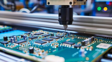
Automated Optical Inspection (AOI): AOI is a powerful tool for detecting issues in the soldering process, such as misaligned components, poor solder joints, or component defects. The earlier you catch these problems, the less likely you’ll need to do time-consuming repairs.
By investing in effective inspection and testing tools, you ensure that faulty units are identified before they reach customers, reducing the need for rework or repairs.

Efficient workflows on the assembly line can also improve PCBA yield and reduce rework. Streamlining operations ensures that each step in the assembly process is completed accurately and consistently, reducing the chance of human error.
Workforce Training: Ensuring that operators are well-trained in assembly processes is crucial. An experienced, knowledgeable team is less likely to make mistakes that could result in defects. Continuous training on best practices and process optimization will contribute to improving yield.
Preventive Maintenance: Regular maintenance of assembly equipment, such as pick-and-place machines, soldering equipment, and testing systems, ensures that they operate correctly and consistently. Equipment failure can lead to defects in the final product, resulting in rework and increased costs.
Lean Manufacturing Principles: Implementing lean manufacturing techniques, such as continuous improvement (kaizen) and root cause analysis, can help identify bottlenecks and inefficiencies in the production line. By eliminating waste and improving process flow, the likelihood of defects decreases, and productivity increases.
Despite all efforts to optimize the design and manufacturing processes, there will inevitably be some defective units that require rework. However, minimizing the need for rework is key to improving overall yield and cost efficiency.
Efficient Rework Process: Having a standardized, well-documented rework process can help minimize the time and cost associated with fixing defects. This may involve specialized tools and techniques for removing and replacing components, correcting soldering issues, or adjusting component placement.
Root Cause Analysis: After rework, it’s essential to conduct a root cause analysis to determine why the defect occurred in the first place. Whether the issue is with the design, materials, or manufacturing process, addressing the underlying cause will help prevent future defects and reduce the need for rework in the long term.

Improving PCBA yield and reducing rework and repair requires a holistic approach that spans the entire manufacturing process. Starting with design optimization (DFM and DFA), selecting quality materials, and refining the soldering process all contribute to better yield. Coupled with rigorous testing and inspection, streamlined workflows, and efficient rework processes, manufacturers can significantly reduce defects and improve efficiency. By focusing on these strategies, electronics manufacturers can lower costs, improve product quality, and deliver reliable, defect-free PCBAs to customers, ultimately boosting their reputation and profitability.
Take Your Projects to New Heights with XPCB Limited
XPCB Limited offers top-notch PCB manufacturing, quick-turnaround prototyping, and turnkey PCBA services designed to make your projects shine. Count on us to bring your ideas to life with efficiency and quality. Your success matters to us, and we’re here to make your innovation journey smooth and rewarding.


XPCB Limited is a premium PCB & PCBA manufacturer based in China.
We specialize in multilayer flexible circuits, rigid-flex PCB, HDI PCB, and Rogers PCB.
Quick-turn PCB prototyping is our specialty. Demanding project is our advantage.
Tel : +86-136-3163-3671
Fax : +86-755-2301 2705
Email : [email protected]
© 2024 - XPCB Limited All Right Reserve
