- +86-755-23012705
- Building 3, Jinfeng Industrial Park, Fuyong Street, Baoan District, Shenzhen ,China
- [email protected]
Copper Thieving refers to the Copper equalizing block added in the outer graphic area of multilayer PCB, PCB assembly auxiliary strip and the manufacturing area of panel auxiliary strip.
What is Copper Thieving good for?
In the process of PCB production, the plating current should be balanced in the process of outer plating process to avoid the uneven copper thickness of the finished product due to the inconsistent current in the plating process. That is, in the process of electroplating, the electroplating current is taken from the copper foil intensive area, so that the current distribution is more even, that is, to avoid the uneven thickness of the finished copper.
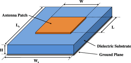
These small copper look like copper clad, but is different, it is made up of many very small independent square shape of copper, copper piece each is independent of the monomer, not with other components for electrical connection in the circuit boards, as we know, for example, large area laying copper on the PCB to focus at least 1/10 of the wavelength frequency spacing too hole metallization, Connect to the main 0V reference plane on PCB. A large area of suspended copper foil is equivalent to Patch Antenna. As shown in the figure below, the common mode current on the board is easy to get into the external electromagnetic radiation and burst, causing EMC problems.

In fact, the high speed digital signal mainly with a low impedance backflow plane PCB outer copper cladding is more harmful than good, note here is “high speed digital signal mainly” and “low impedance backflow plane”, pay attention to this presupposition, if it is a double-layer plate or high impedance analog circuit, copper cladding is very good.

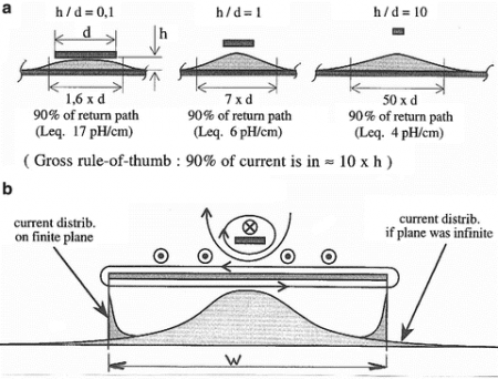
For multilayer PCB has low impedance back plane, the high number of digital signal backflow will directly go minimum impedance shortest paths rather than linear distance to the path of least resistance, which is most reflow focused on signal corresponding to the reference plane, go line and the reference plane at a distance of H is smaller, back on the reference plane of the current focus on running with the corresponding area, In other words, the area of reflux current diffusion is relatively small, which can reduce crosstalk. The closer the reflux coupling is, the less the differential mode radiation can be reduced. So, to improve the performance of the surface of EMC optimization method is through reasonable laminated structure design, make the reference for the signal transmission line and plane, as close as possible to return from the low impedance of the reference plane, rather than through the way of laying copper structure also return path to make up for, that is not what happened to copper clad. To cover copper, you also need to make metallization holes to connect to the 0V reference plane, in corners of the place, copper can easily form an accidental antenna. Once played holes, each hole crowding the lining of the already crowded go line space, and the integrity of the main power / 0 v reference plane, was more and more IC pins and go line in layer hole has taken the plane as the screen mesh, plus the outer plane to fill the pile hole, to the detriment of the principal plane of low impedance more. At the same time, improper processing of copper foil will cause a sudden change in the impedance of the transmission line if it is too close to the transmission line requiring control impedance in the local area, and signal reflection will be generated where the impedance is discontinuous, causing signal integrity problems.

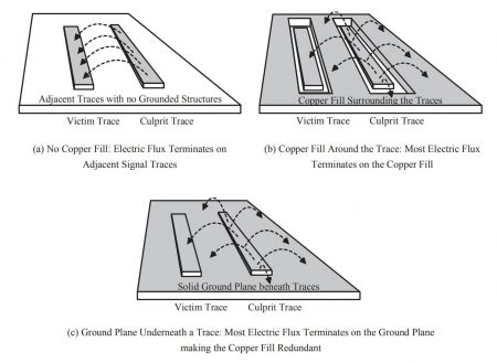
Of course, if there is relatively complete copper foil in the outer layer, these copper foil can play a shielding role to some extent, or can improve the interlayer capacitance of PCB, which will be helpful to improve the EMC performance. However, in the case of high digital signals, the outer layer is covered with components and fan holes, so it is difficult to form a complete plane. At the same time, the 0V reference plane needs to be wiring, so it is difficult to ensure the integrity of the plane. At this time, laying copper in the empty place of the board and punching more holes to connect with the 0V reference to construct low impedance reflow path is very beneficial to improve the EMC performance. For the high-number digital signal wiring area with low impedance reference plane, Wu does not put copper on the outer layer. However, if the residual copper rate in the outer layer is too low, such as the main control area and surrounding DRAM and other BGA areas, the density of copper foil is relatively dense, while the copper content in other areas is relatively small. The uneven copper distribution rate is in the electroplating process. The current density through BGA area is too large, resulting in uneven copper thickness of electroplating finished products, such as difference line, uneven copper thickness will have a negative impact on impedance control, and the large difference of copper thickness on BGA pins will also have an impact on SMT yield.
The solution is to improve the distribution of the copper foil density balance, the small chess lattice copper is a good choice, of course, also have a plenty of small dot shapes, each of its monomer is far much smaller in physical size of a quarter, it is difficult to form effective radiating antenna, without a reference plane connection hole at 0 v, don’t have to use the lining of the crowded go line space, The only thing to be noted is that there should be no impedance control line at the bottom of Copper Thieving, as these Copper blocks will cause impedance discontinuity. Of course, don’t get too close to areas that need ESD protection.
The plate factory will add balance copper blocks for you according to the residual copper rate calculated by CAM software and send you for confirmation. At this time, it is necessary to pay attention to check whether these copper blocks will have a negative impact on the impedance. Of course, it is better to add them by yourself to avoid any deviation in communication with the process personnel of the plate factory, such as the version after Cadence Allegro 16.6. Mentor Pads Professional and other mainstream EDA software have added the function of adding Copper Thieving.
Copper Thieving refers to the Copper in the outer layer, Thieving is to steal plating current to make the outer layer of Copper plating more uniform, the same Copper in the inner layer, there is no Thieving, this is the balance of Copper. Avoid the inner layer resin area is too large when the inner layer is pressed together, resulting in cavities or bubbles, and balance the mechanical stress difference produced when different layers of copper foil are heated. The copper block is still the same copper block, but it does a different job.


XPCB Limited is a premium PCB & PCBA manufacturer based in China.
We specialize in multilayer flexible circuits, rigid-flex PCB, HDI PCB, and Rogers PCB.
Quick-turn PCB prototyping is our specialty. Demanding project is our advantage.
Tel : +86-136-3163-3671
Fax : +86-755-2301 2705
Email : [email protected]
© 2024 - XPCB Limited All Right Reserve
