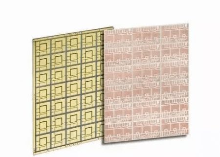
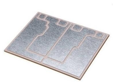
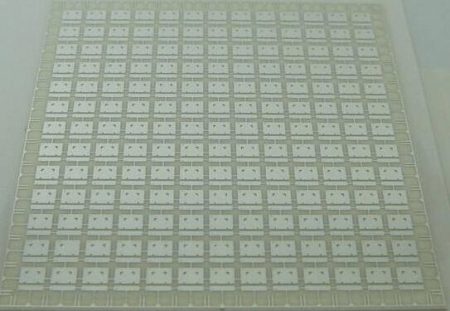
Ceramic substrate refers to copper foil at high temperature directly bonded to aluminum oxide (Al2O3) or aluminum nitride (AlN) ceramic substrate surface (single or double) special process plate. The ultra-thin composite substrate has excellent electrical insulation performance, high thermal conductivity, excellent soft brazing property and high adhesion strength, and can etch all kinds of graphics just like PCB board, with great current carrying capacity. Therefore, ceramic substrate has become the basic material of high power electronic circuit structure technology and interconnection technology.
Ceramic substrate characteristics
- Strong mechanical stress and stable shape; High strength, high thermal conductivity, high insulation; Strong adhesion, anti-corrosion.
- Excellent thermal cycling performance, up to 50,000 cycles, high reliability.
- The structure of various graphics can be etched as PCB board (or IMS substrate); No pollution, no pollution.
- The service temperature is -55℃ ~ 850℃; The thermal expansion coefficient is close to silicon, which simplifies the production process of the power module.

The advantage of ceramic substrate
- The thermal expansion coefficient of ceramic substrate is close to that of the silicon chip, which can save transition layer Mo sheet, save labor, material and cost;
- Reduce welding layer, reduce thermal resistance, reduce cavity and improve yield;
- Under the same load flow, the width of 0.3mm thick copper foil wire is only 10% of that of an ordinary printed circuit board;
- Excellent thermal conductivity makes the package of the chip very compact, thus greatly increasing the power density and improving the reliability of the system and device;
- Ultra-thin ceramic substrate (0.25mm) can replace BeO without environmental toxicity;
- Large carrying capacity, 100A current continuously passes through 1mm wide 0.3mm thick copper body, and the temperature rise is about 17℃; The current of 100A continuously passes through 2mm wide 0.3mm thick copper body, and the temperature rise is only about 5℃.
- Low thermal resistance. The thermal resistance of ceramic substrates with a thickness of 0.63mm is 0.31k /W, that of ceramic substrates with a thickness of 0.38mm is 0.19k /W, and that of ceramic substrates with a thickness of 0.25mm is 0.14k /W.
- High insulation pressure, to ensure personal safety and equipment protection ability.
- New packaging and assembly methods can be implemented to make products highly integrated and smaller in size.

The difference between ceramic substrate and ordinary PCB
At present, the FR-4 circuit board is widely used in the market, but the FR-4 circuit board defect is irreversible.
The technical staff of XPCB Ltd. made a simple analysis of the circuit boards on the market with their years of experience in making circuit boards.
Advantages of FR-4 copper clad laminate:
- Do not use insulation
- Mass production
- Fast molding
- Low prices
There are almost twelve kinds of defects:
- 1.thickness deviation is more common in the thick around the thin, or thick side, thin side. It will affect the processing of PCB, uneven thickness will affect the depth of grooving. Substrate selectivity. For the more precise printed circuit board, the thick plate out of tolerance will cause the whole machine when the plug is not elastic, forming bad contact. Affect the performance of electronic devices. For multilayer printed circuit boards: The accumulation of thickness error may result in the whole piece of plate thickness error resulting in waste products. Can not meet the test platform and other high precision products to the high pressure plate thick bottom tolerance requirements.
- Substrate flowage: it affects the welding resistance, electrical insulation and many other properties of the substrate, so it cannot be used as a genuine product.
- Substrate stratification: there is this phenomenon is not impossible to apply, but can not become A grade A product.
- White spot on the substrate.White lines: seriously affect PCB manufacturing quality.
- Substrate dew pattern: cause insulation performance degradation, seriously affect the QUALITY of PCB board.
- Substrate impurities.Black spot: There are other effects besides the appearance of the product, what can be done now is.
- Copper foil folding: Those with such creases are not allowed to be used in PCB production.
- Glue point: It is a cured resin. During the making process, the corrosion does not fall off. Seriously affect the insulation between the wires. Therefore, it cannot be used for PCB production.
- Pit: it has a great impact on PCB product quality, which may cause circuit failure or disconnection.
- Pinhole: it will cause a rough picture, there are traces of kerosene leakage.
- Copper foil oxidation: Slight oxidation will not affect PCB product quality, but it should be prevented as far as possible. Serious oxidation may cause PCB production process is not easy to corrosion clean, can not be used in copper-clad laminate production.
- Copper foil highlights: due to the damage of the antioxidant layer, the spot is easy to be oxidized in the storage process of the product, causing adverse effects on PCB. For larger highlights, copper-tin may be thinner than other places, but also affect the PCB manufacturing quality.
Advantages of ceramic circuit board:
- Higher thermal conductivity
- Better matching coefficient of thermal expansion
- A hard, low resistance of the metal film alumina ceramic circuit board
- Good solderability and high temperature of the base material.
- Good insulation
- Low-frequency loss
- Assembly with high density
- No organic ingredients, resistant to cosmic rays, high aerospace reliability, long service life
- The copper layer does not contain an oxide layer, can be used in reducing the atmosphere for a long time.

Disadvantages of ceramic circuit board:
- Fragile: this is the main one of the shortcomings, can only make a small area of the circuit board.
- High price: There are more and more requirements for electronic products. Ceramic circuit board can only meet some high-end products, and low-end products will not be used at all.

So the question is, what is the value of ceramic PCB? It is analyzed from the following three aspects:
- Substrate materials: ceramic PCB currently has two main types of aluminum oxide and aluminum nitride, and the cost of these two materials is much more expensive than resin substrate or aluminum substrate, copper substrate. From the base, the price has been pulled apart.
- Process technology: From the perspective of manufacturing technology, no matter LTCC, HTCC, DPC, DBC or LAM, their manufacturing process will require high requirements, and the joint burning temperature required by LTCC and HTCC is difficult to control.
- Product performance: As the saying goes, “you get what you pay for”, which is vividly demonstrated on ceramic PCB. PCB has many important demand points, such as thermal conductivity, thermal expansion coefficient, dielectric constant, stability, high-frequency loss, etc.
In these aspects, ceramic PCB can achieve the current top. Its thermal conductivity is the best among THE PCB at present, and its thermal expansion coefficient is more compatible with the silicon chip, with very low dielectric constant, excellent electrical conductivity, corrosion resistance, high-temperature resistance, and small loss at high frequency.
