- +86-755-23012705
- Building 3, Jinfeng Industrial Park, Fuyong Street, Baoan District, Shenzhen ,China
- [email protected]
High-Density Interconnect (HDI) Printed Circuit Boards (PCBs) are increasingly being used in high-end applications such as smartphones, wearables, automotive electronics, medical devices, and telecommunications equipment. HDI PCBs are known for their ability to accommodate a large number of components in a small space, while maintaining excellent signal integrity and performance. The assembly process of HDI PCBs, however, is more complex than that of traditional PCBs due to their smaller size, finer pitch components, and multilayer structure. In this blog, we will analyze the key technologies involved in the assembly process of HDI PCBs for high-end applications.
HDI PCBs are advanced circuit boards that have a higher density of components and interconnections compared to conventional PCBs. They typically use fine lines and spaces, small vias (microvias), and advanced materials to support high-performance electronic devices. The key feature of HDI PCBs is their ability to support high-density component placement while maintaining small form factors and improved signal integrity.
These boards are ideal for high-end applications that require miniaturization, high-speed performance, and reliability. They are commonly used in devices like smartphones, tablets, wearables, automotive electronics, and high-frequency communication equipment, where space is limited, but performance and reliability are crucial.
One of the most significant differences between traditional PCBs and HDI PCBs is the use of microvias. Microvias are very small holes that connect layers within the PCB. They are typically created using laser drilling or mechanical drilling methods, allowing for precise and high-density interconnections between layers.
Laser Drilling: Laser drilling technology is used to create microvias with very fine diameters, usually in the range of 50 to 100 microns. This is crucial for HDI PCBs as it allows for high-density routing and component placement without increasing the size of the PCB.
Stacked Microvias: In more advanced HDI designs, stacked microvias (or blind vias) are used to connect multiple layers. Stacked vias save space by enabling vertical connections between layers, which is essential for high-performance devices that need to minimize size.
The precision of microvia technology directly affects the reliability and performance of the final product. Improperly drilled microvias can lead to poor electrical connections, signal degradation, and ultimately, product failure.

HDI PCBs are typically used for applications that require fine-pitch components, such as Ball Grid Arrays (BGAs), Chip-on-Board (COB) packages, and small-outline integrated circuits (SOICs). These components have very small lead pitches (the distance between the leads), which require advanced assembly techniques.
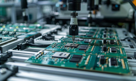
Pick-and-Place Machines: Automated pick-and-place machines are essential for handling fine-pitch components. These machines use high-precision vision systems and robotic arms to place components accurately on the PCB. The ability to place components with sub-millimeter precision is crucial in HDI PCB assembly to avoid misplacement and short circuits.
Solder Paste Printing: The accuracy of solder paste deposition is critical in the assembly of fine-pitch components. Automated solder paste printers apply solder paste to the PCB pads before component placement. The paste must be applied precisely, especially for small components, to ensure strong and reliable solder joints. Improper paste application can result in defects like solder bridging, which can cause short circuits or poor electrical connections.
Reflow soldering is the standard method used to attach components to HDI PCBs. In this process, solder paste is heated to its melting point in a reflow oven, where it forms a solid bond between the PCB pads and component leads. However, because HDI PCBs often feature small and dense components, reflow soldering requires careful control to avoid defects.
Temperature Profile Control: Reflow ovens used in HDI PCB assembly must be carefully calibrated to ensure that temperature profiles are optimized for the small and densely packed components. The oven needs to provide a gradual increase in temperature, followed by a cooling period to solidify the solder. Any temperature irregularities can lead to soldering issues such as cold joints or solder bridges, which would compromise the board’s reliability.
Selective Soldering for Through-Hole Components: While HDI PCBs primarily use surface-mount technology, they may still contain a few through-hole components. Selective soldering machines are used to solder through-hole components without affecting the delicate surface-mount components. This process is highly precise and minimizes the risk of damaging small components.

The high-density nature of HDI PCBs and the fine-pitch components they contain make inspection and quality control critical. Automated Optical Inspection (AOI) and X-ray inspection are two key techniques used to ensure the integrity of HDI PCB assemblies.
Automated Optical Inspection (AOI): AOI systems use cameras and image processing software to visually inspect solder joints, component placement, and overall board integrity. For HDI PCBs, AOI machines must have high-resolution cameras to detect minute defects such as misaligned components, insufficient solder, or solder bridges. These machines can detect errors early in the production process, reducing the risk of defects in the final product.
X-ray Inspection: X-ray inspection is essential for inspecting hidden solder joints, particularly for BGAs, which have solder balls underneath the component. X-ray systems can inspect the quality of the solder connections without damaging the PCB. This is particularly important for high-end applications where reliability is critical, such as in medical devices or aerospace systems.
The choice of materials used in HDI PCBs is another crucial factor for ensuring performance and reliability, especially in high-end applications. For example, the use of high-frequency materials (such as PTFE) is common in applications like telecommunications and RF devices. Additionally, the use of high-temperature-resistant materials ensures that the PCB can withstand the harsh environments of automotive and industrial applications.
Thermal Cycling Testing: To assess the reliability of HDI PCBs, thermal cycling tests are performed to simulate the extreme temperature changes the board may experience during its lifetime. This helps identify potential issues with component bonding or material expansion.
High-Frequency Testing: For high-end applications such as RF and microwave communication, testing for signal integrity is crucial. HDI PCBs are designed to minimize signal loss, but the quality of the PCB assembly can still be affected by issues like impedance mismatch or poor solder joints.

HDI PCBs play a vital role in high-end applications that demand compact size, high performance, and reliability. The assembly process of these advanced boards requires precision and expertise in various key technologies, including microvia technology, fine-pitch component placement, reflow soldering, advanced inspection techniques, and material selection. As the demand for smaller, more powerful electronic devices continues to grow, HDI PCBs will remain at the forefront of technological innovation, enabling the next generation of high-performance, space-efficient devices. Ensuring the success of their assembly process is essential for maintaining the quality and reliability that high-end applications require.
Your Trusted Partner for PCB Success: XPCB Limited
Let XPCB Limited be your guide to PCB success. Our comprehensive PCB manufacturing, rapid prototyping, and turnkey PCBA services are designed to meet your needs with ease. Count on us to deliver reliable solutions that exceed your expectations. With XPCB Limited, your journey to PCB excellence starts here.


XPCB Limited is a premium PCB & PCBA manufacturer based in China.
We specialize in multilayer flexible circuits, rigid-flex PCB, HDI PCB, and Rogers PCB.
Quick-turn PCB prototyping is our specialty. Demanding project is our advantage.
Tel : +86-136-3163-3671
Fax : +86-755-2301 2705
Email : [email protected]
© 2024 - XPCB Limited All Right Reserve
