The rapidly evolving world of technology demands innovative and high-performing electronic solutions. Multilayer Printed Circuit Boards (PCBs) and High-Density Interconnect (HDI) PCBs have become pivotal in meeting these demands, offering compact, reliable, and high-speed solutions for a myriad of applications. This blog delves into the intricacies of multilayer PCB assembly and HDI PCB manufacturing, exploring their significance, applications, and the processes involved.
What Are Multilayer PCBs?
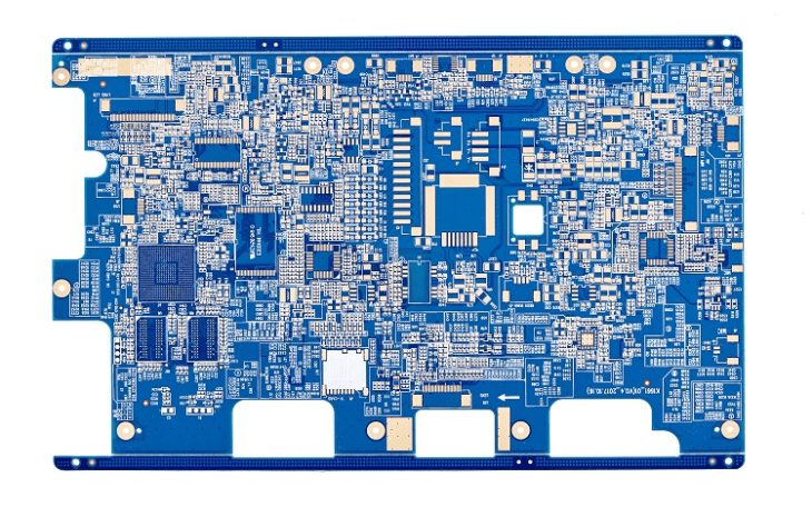
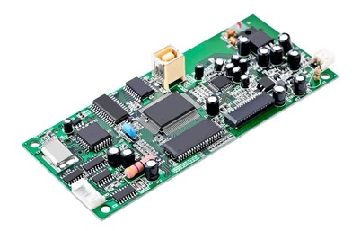
Multilayer PCBs consist of three or more conductive layers stacked together, separated by insulating materials. Unlike single or double-sided PCBs, multilayer boards provide increased circuit density and functionality within a compact design. These PCBs are essential for devices requiring complex and high-speed circuits.
Key features of multilayer PCBs include:
- Compact Design: Multiple layers reduce the overall size of the board, ideal for portable and space-constrained devices.
- High Performance: Enhanced functionality supports advanced computing and communication requirements.
- Improved Signal Integrity: Layer stacking reduces electromagnetic interference (EMI) and enhances signal quality.
What Are HDI PCBs?
HDI PCBs take PCB design to the next level by incorporating advanced features such as:
- Microvias: Extremely small vias that allow interconnectivity between layers.
- Blind and Buried Vias: Vias that connect specific layers without passing through the entire board.
- Thin and Lightweight Design: Ideal for modern high-tech gadgets.
- High Component Density: Increased wiring density supports complex circuits within a small footprint.
HDI PCBs are a natural evolution of multilayer PCBs, designed to meet the demands of high-speed communication, compact electronics, and high-frequency performance.
The Importance of Multilayer and HDI PCBs
Multilayer and HDI PCBs are integral to industries that require precision, performance, and miniaturization. Some benefits include:
- Space Efficiency Multilayer and HDI PCBs optimize space utilization, enabling the integration of more components within a smaller area. This is critical for portable devices like smartphones, tablets, and wearables.
- Enhanced Functionality With the ability to support complex circuits, these PCBs are ideal for advanced applications such as IoT devices, high-speed data processing, and AI-driven technologies.
- Reliability and Durability Advanced manufacturing techniques ensure robust PCBs capable of withstanding harsh environmental conditions, making them suitable for aerospace, automotive, and medical applications.
- Improved Performance Features like reduced EMI, high signal integrity, and low power consumption make multilayer and HDI PCBs indispensable for high-speed and high-frequency applications.
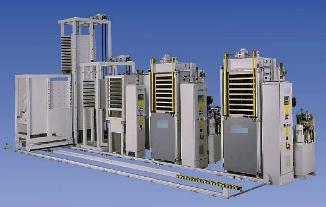
The Manufacturing Process: From Concept to Reality
Multilayer PCB assembly and HDI PCB manufacturing involve meticulous planning and execution. Here’s a step-by-step overview:
- Design and Prototyping The process begins with the creation of a detailed design using Computer-Aided Design (CAD) tools. Factors like layer count, material selection, and via types are finalized. Prototyping allows for testing and validation before mass production.
- Material Preparation High-quality substrates, copper foils, and prepregs (insulating layers) are selected based on the application requirements. Materials like FR-4, polyimide, or Rogers laminates are commonly used.
- Layer Stacking and Lamination In multilayer PCBs, the conductive and insulating layers are stacked together and laminated under heat and pressure. For HDI PCBs, advanced techniques like sequential lamination are employed to incorporate microvias and blind/buried vias.
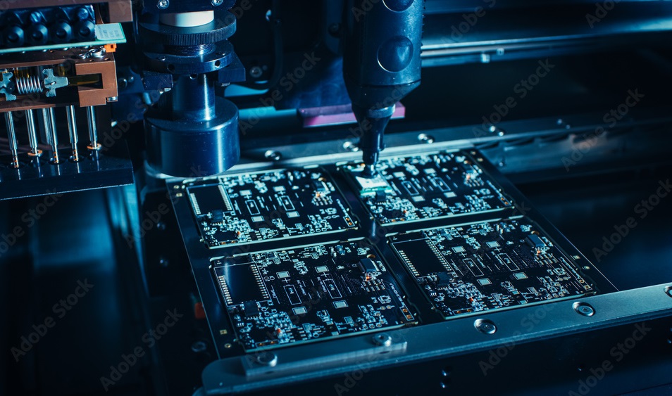
- Drilling and Via Formation Precision drilling equipment creates holes for vias, which are plated with conductive materials to establish electrical connections. Laser drilling is commonly used for microvias in HDI PCBs.
- Etching and Patterning Chemical etching removes unwanted copper, leaving behind the desired circuit patterns. HDI PCBs require advanced etching techniques to achieve fine line widths and spacing.
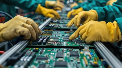
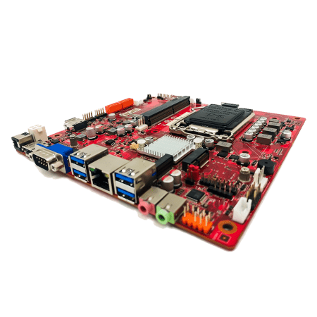
- Component Assembly Surface Mount Technology (SMT) is used to assemble components onto the PCB. Automated pick-and-place machines ensure accuracy, while reflow soldering creates reliable connections.
- Inspection and Testing Rigorous testing, including Automated Optical Inspection (AOI), X-ray inspection, and functional testing, ensures the PCBs meet quality and performance standards.
Applications of Multilayer and HDI PCBs
The versatility and high performance of multilayer and HDI PCBs make them indispensable in various industries, including:
- Consumer Electronics: Smartphones, laptops, gaming consoles, and wearables.
- Automotive: Advanced Driver Assistance Systems (ADAS), infotainment, and electric vehicle components.
- Medical Devices: Imaging systems, diagnostic equipment, and portable health monitors.
- Aerospace and Defense: Navigation systems, communication devices, and avionics.
- Telecommunications: 5G infrastructure, high-speed routers, and satellite communication equipment.
Choosing the Right Manufacturing Partner
Partnering with a reliable PCB manufacturer is crucial to achieving optimal results. Here are some factors to consider:
- Experience and Expertise: Choose a manufacturer with a proven track record in multilayer and HDI PCB production.
- Technological Capabilities: Ensure they use state-of-the-art equipment and follow industry best practices.
- Quality Standards: Look for certifications like ISO 9001, IPC-A-610, and UL to guarantee quality and reliability.
- Customization and Support: A good partner should offer design assistance, prototyping, and end-to-end support.
Conclusion
Multilayer PCB assembly and HDI PCB manufacturing are at the forefront of technological innovation, enabling the development of cutting-edge electronic solutions. By leveraging these advanced PCB technologies, businesses can create compact, efficient, and high-performing devices that meet the demands of today’s competitive markets.
Whether you’re designing next-generation consumer electronics or critical medical devices, multilayer and HDI PCBs offer the precision and reliability you need. Partner with a trusted PCB manufacturer to bring your high-tech visions to life and stay ahead in the rapidly evolving world of electronics.
At XPCB Limited, we’re here to help you explore new horizons. Our advanced PCB manufacturing, rapid prototyping, and turnkey PCBA solutions make it easy for you to turn your ideas into reality. Trust us to deliver excellence and reliability every step of the way. Join us and experience the power of innovation with XPCB Limited by your side.