- +86-755-23012705
- Building 3, Jinfeng Industrial Park, Fuyong Street, Baoan District, Shenzhen ,China
- [email protected]
In the world of electronics, the importance of printed circuit boards (PCBs) cannot be overstated. These essential components serve as the backbone of electronic devices, ensuring that all the components are properly connected and functional. Among the various types of PCBs available, multilayer rigid PCBs stand out due to their complexity, durability, and efficiency. This blog will explore the process of multilayer rigid PCB manufacture and assembly, highlighting the precision and innovation involved.
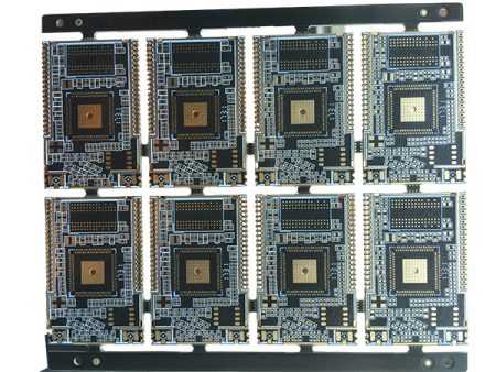
A multilayer rigid PCB is a type of PCB that contains more than two conductive layers separated by insulating materials. These boards typically have three or more layers of copper, and each layer is connected to the others using vias, which are small holes through which electrical signals pass. The rigid part refers to the board’s material, which is hard and unyielding, as opposed to flexible PCBs that can bend and twist.
Multilayer rigid PCBs are used in applications where high performance, compact size, and reliability are crucial. These boards can be found in everything from smartphones, computers, and medical devices to aerospace systems and automotive electronics.

The manufacture of multilayer rigid PCBs involves several intricate steps, each requiring precision and advanced technology. Let’s break down the process:
Before any physical production begins, a detailed PCB design is created using specialized software. Designers need to plan the layers of the PCB, the copper trace widths, and the component placement. This design phase is crucial because any error can lead to defects in the final product, which could affect the functionality of the entire device.
Once the design is finalized, it is sent to the manufacturer for production.
In the case of multilayer PCBs, multiple layers of copper foil are stacked together with layers of insulating material, typically made of epoxy resin. Each layer is etched with the required circuit patterns using a chemical etching process, removing the copper where it’s not needed, leaving behind traces that will form the electrical connections.
After each layer has been prepared, they are stacked together, with a layer of prepreg (pre-impregnated resin) placed in between. The stack is then subjected to heat and pressure in a lamination press, which bonds the layers together. The result is a single solid PCB with multiple conductive layers. The number of layers depends on the complexity of the design.
To allow for electrical connections between the different layers, tiny holes called vias are drilled into the PCB. Vias are used to connect the different layers of the PCB, allowing signals to pass from one layer to another. There are different types of vias—blind vias (which connect outer layers to internal layers), buried vias (which connect only internal layers), and through-hole vias (which pass from one side of the PCB to the other).
The drilling process requires precision and specialized equipment to ensure the vias are in the correct locations and the right size.
After drilling, the vias are plated with copper to create electrical pathways between the layers. Once the plating is done, the PCB goes through a solder masking process. A thin layer of solder mask is applied to the surface of the PCB to protect the copper traces from corrosion, reduce short circuits, and prevent solder from bridging between components during assembly. The solder mask also gives the PCB its distinctive green color.
Next, the surface of the PCB is treated to ensure that it is ready for soldering. A variety of finishes, including HASL (Hot Air Solder Leveling), ENIG (Electroless Nickel Immersion Gold), and OSP (Organic Solderability Preservative), can be used depending on the requirements of the design. These finishes provide a durable, reliable surface for the components to be soldered onto.
Quality control is crucial at every step of PCB manufacturing. Once the multilayer PCB is fully assembled, it undergoes rigorous testing to ensure all electrical connections are intact and that the board functions as expected. Common testing methods include automated optical inspection (AOI), electrical testing, and X-ray inspection for checking the vias and internal layers.

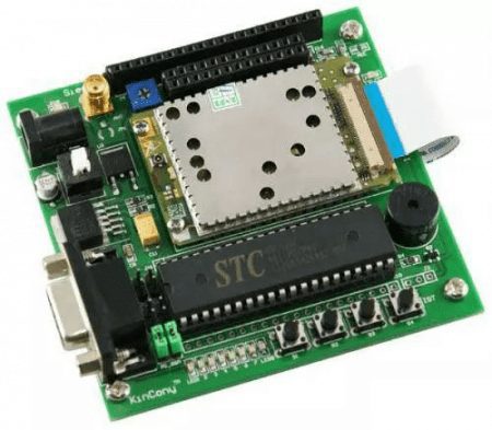
Once the multilayer rigid PCB is manufactured, the assembly process begins. This is where the actual electronic components (resistors, capacitors, ICs, etc.) are soldered onto the board. The assembly process can be broken down into two main methods: surface-mount technology (SMT) and through-hole technology (THT).
SMT is the most common method for placing components on a PCB. In this process, the components are mounted directly onto the surface of the PCB. First, solder paste is applied to the PCB in the locations where components will be placed. Then, components are positioned on the paste using automated pick-and-place machines. The board is passed through a reflow oven, where the solder paste melts and creates a solid connection between the components and the PCB.
For components that require a more secure mechanical connection, THT is used. This process involves inserting component leads through holes in the PCB, which are then soldered on the opposite side. THT is typically used for components that need higher durability or for components that require a more robust physical connection, such as connectors and large capacitors.
After the assembly is complete, the PCB goes through another round of rigorous testing. Functional testing ensures that the PCB works as intended, while visual inspections check for any soldering issues or component placement errors. If the PCB passes all tests, it is ready for use in the final product.
The demand for smaller, faster, and more efficient electronic devices has driven innovation in PCB manufacturing. Multilayer rigid PCBs have become increasingly complex, incorporating advanced features such as microvias, HDI (High-Density Interconnect) designs, and integrated passive components. These innovations enable manufacturers to produce boards with higher component density, improved performance, and reduced size, which are crucial for modern electronics.
The use of advanced materials and automated production processes has also significantly improved the efficiency and cost-effectiveness of multilayer PCB manufacturing. As electronic devices become more sophisticated, the evolution of PCB technology continues to play a key role in pushing the boundaries of what is possible in electronics.

The manufacture and assembly of multilayer rigid PCBs is a complex, highly precise process that requires a combination of advanced technology, skilled labor, and strict quality control. From the design phase to the final testing and assembly, every step is crucial in ensuring that the PCB meets the performance, durability, and reliability standards required by modern electronic devices.
As technology continues to advance, multilayer rigid PCBs will remain at the heart of innovation in electronics, enabling the development of more powerful, compact, and efficient devices. Whether it’s for consumer electronics, medical equipment, or aerospace systems, the precision and innovation involved in PCB manufacturing will continue to shape the future of electronics.
Take Your Projects to New Heights with XPCB Limited
XPCB Limited offers top-notch PCB manufacturing, quick-turnaround prototyping, and turnkey PCBA services designed to make your projects shine. Count on us to bring your ideas to life with efficiency and quality. Your success matters to us, and we’re here to make your innovation journey smooth and rewarding.


XPCB Limited is a premium PCB & PCBA manufacturer based in China.
We specialize in multilayer flexible circuits, rigid-flex PCB, HDI PCB, and Rogers PCB.
Quick-turn PCB prototyping is our specialty. Demanding project is our advantage.
Tel : +86-136-3163-3671
Fax : +86-755-2301 2705
Email : [email protected]
© 2024 - XPCB Limited All Right Reserve
