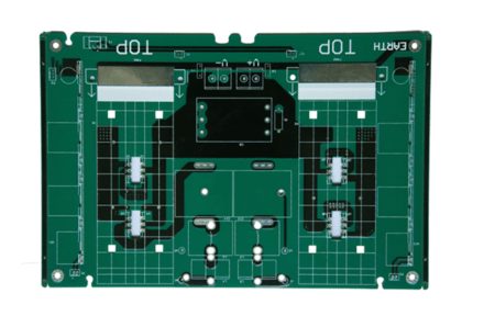
With the development of electronic products to high density and high precision, the same requirements are put forward for circuit boards, which makes circuit boards gradually develop in the direction of HDI. The most effective way to increase PCB density is to reduce the number of through-holes, and accurately set blind holes and buried holes.

1. The Definition of HDI Blind Hole Plate
- In contrast to through holes, through holes refer to holes drilled through each layer, and HDI blind holes are non-drilled through holes.
- The subdivision of HDI blind hole: blind hole (BLIND HOLE), buried hole (BURIED HOLE) (outer layer is not visible);
- Distinguish from the HDI circuit board production process: blind holes are drilled before pressing, while through holes are drilled after pressing.
2. The Manufacturing Method of Circuit Board
A: Drill Belt:
- Select reference point: select the through hole (i.e. a hole in the first drill belt) as the unit reference hole.
- Each blind hole drilling belt needs to be selected a hole and marked the coordinates relative to the unit reference hole.
- Pay attention to the corresponding layers: the unit sub-hole diagram and drill bit table must be marked, and the names of the front and back must be the same; the sub-hole diagram cannot demenstrated with abc, while the front is indicated by 1st, 2nd.
Note that whether the laser hole is sleeved with the inner buried hole, or whether the holes of the two drill belts are at the same position.
B: The Production of pnl Board Edge Process Hole:
Ordinary PCB multi-layer circuit board: the inner layer is not drilled;
- The rivets gh, aoigh, etgh are all shot after the board is eroded (die-cut).
- Target hole (drilled hole gh) ccd: the outer layer needs to be copper out
- X-ray machine: it needs to be directly punched out, and noted that the long side is at least 11 inches.
All tooling holes should be drilled.Pay attention to rivets gh,which needs to be out to avoid misalignment(Aoigh is also die-cut).The edge of the pnl board needs to be drilled to distinguish each board.
3. The Modification of Films
Note that the film is produced positive and negative:
- General principle: HDI circuit board thickness is greater than 8mil (without copper connection) to follow the positive film process;
- The thickness of the circuit board is less than 8mil (without copper) and the negative film process (thin board);
- When the line thickness and the line gap are large, the copper thickness at d/f should be considered, not the bottom copper thickness.
- The blind hole ring can be made 5mil instead of 7mil.
- The inner independent pad corresponding to the blind hole needs to be retained.
- Blind holes cannot be made without ring holes.


