- +86-755-23012705
- Building 3, Jinfeng Industrial Park, Fuyong Street, Baoan District, Shenzhen ,China
- [email protected]
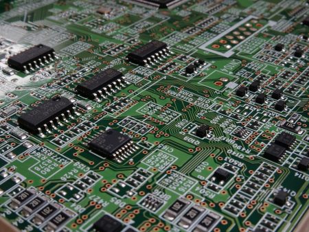
In the realm of electronics manufacturing, ensuring the reliability and functionality of printed circuit board assemblies (PCBA) is critical. The PCBA testing process is a systematic approach designed to identify defects and verify that the assembly meets design specifications. This blog will explore the key steps involved in the PCBA testing process and highlight important considerations at each stage.
The testing process begins with a thorough visual inspection of the PCBA. This step aims to identify any physical defects that could impact performance.
Key Points:
Check for proper placement of components and ensure that polarities are correct.
Look for any signs of damage, such as scratches, dents, or discoloration.
Inspect solder joints for quality, ensuring there are no cold solder joints, shorts, or open circuits.
Visual inspection serves as the first line of defense against obvious issues and is essential for ensuring that the board is ready for further testing.

Once the visual inspection is complete, the next step is to conduct electrical tests. This involves checking the integrity of the circuit pathways.
Purpose: Ensure that electrical connections are intact.
Key Points: Use a multimeter to check for continuity across traces and between pads to confirm that there are no open circuits.
Purpose: Assess the signal integrity of the PCB.
Key Points: Measure the impedance to ensure it falls within the specified range, reducing the risk of signal reflections that can lead to performance issues.
Purpose: Verify that the PCBA performs as intended.
Key Points: Test each function of the assembly according to the design specifications. This may involve checking the output signals, response times, and overall functionality of the assembled product.
Burn-in testing is conducted to simulate long-term use of the PCBA under stress conditions.
Key Points:
Expose the PCBA to elevated temperatures and voltages for a specified duration.
Monitor performance to identify any early failures, ensuring the reliability of the assembly before it reaches the end user.

To ensure that the PCBA can withstand various operating conditions, environmental testing is crucial.
Purpose: Assess performance under extreme temperature changes.
Key Points: Cycle the PCBA through high and low temperatures to check for physical and electrical reliability.
Vibration Testing:
Purpose: Ensure structural integrity in environments with mechanical stress.
Key Points: Subject the PCBA to vibrations that mimic real-world conditions, assessing its durability.
Quality of solder joints is vital for the reliability of PCBA.
Key Points:
Utilize automated optical inspection (AOI) or X-ray inspection to examine solder joints.
Ensure that joints are uniform and adequately formed to prevent future failures.
The last step in the testing process involves comprehensive functional verification to confirm that the final product meets all operational requirements.
Key Points:
Perform a series of tests that mimic end-user conditions to validate the product’s performance in real-world applications.
Document any anomalies and ensure all functional requirements are met before shipping.
Finally, thorough documentation of the testing process is essential for quality assurance and traceability.
Key Points:
Maintain detailed records of all tests performed, including results and any corrective actions taken.
This documentation not only supports quality control but also aids in future troubleshooting and product improvements.

The PCBA testing process is a critical component of electronics manufacturing, ensuring that products are reliable and meet design specifications. By following a systematic approach that includes visual inspections, electrical testing, burn-in testing, environmental assessments, solder quality inspections, final verifications, and meticulous documentation, manufacturers can significantly reduce the risk of failures and enhance product quality. As technology continues to advance, robust testing processes will remain essential to maintaining trust in electronic products.
Make Your PCB Dreams a Reality with XPCB LimitedXPCB Limited is your go-to partner for turning your PCB dreams into reality. Our streamlined PCB manufacturing process, combined with quick-turnaround prototyping and turnkey PCBA services, ensures that your projects come to life with ease. Trust in our expertise and dedication to quality as we help you achieve your PCB goals. Join us and experience the difference with XPCB Limited.


XPCB Limited is a premium PCB & PCBA manufacturer based in China.
We specialize in multilayer flexible circuits, rigid-flex PCB, HDI PCB, and Rogers PCB.
Quick-turn PCB prototyping is our specialty. Demanding project is our advantage.
Tel : +86-136-3163-3671
Fax : +86-755-2301 2705
Email : [email protected]
© 2024 - XPCB Limited All Right Reserve
