What problems need to be paid attention to in SMT mass processing and production?
With the continuous development of high technology, many electronic devices are becoming thinner and smaller, which makes many SMD electronic components smaller and smaller.
- To carry out SMT chip processing, it must be applied to solder paste, and if the solder paste just purchased is not applied immediately, it must be placed in a natural environment of 5-10 degrees, and the temperature must not be less than 0 degrees or higher than 10 degrees.
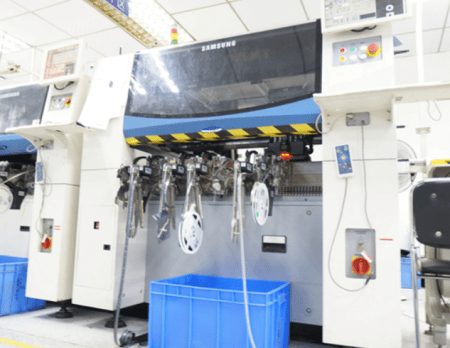
- Daily maintenance of SMT machinery and equipment: SMT machine equipment should be maintained on time, and the rules and regulations of equipment inspection should be improved. Suppose the machinery and equipment are embrittled, or the components are damaged. In that case, there will be a series of conditions such as patch crookedness and high material throwing, which will seriously affect the production and manufacturing.
- Improvement and setting of the main parameters of the processing technology: In order to ensure the quality of the PCB board electric welding, we must always pay attention to whether the basic parameters of the processing technology of the reflow oven are effective. Under normal circumstances, the temperature control should be tested twice a day, and only by continuously improving the temperature curve can the quality of the products produced and processed be ensured.

- Improve the inspection method: the complexity of the structure and processing technology of electronic components has put forward high requirements for non-destructive testing technology, and the basic inspection methods such as visual inspection method, automatic electron-optical inspection method (AOI), electrical testing method (ICT), and ultrasonic testing method have long been unable to meet the requirements of relative density, efficient operation and standardization in the field of SMT. X-ray inspection is the best choice to improve the quality of inspection and manufacturing at this stage.
What links need to be paid attention to in the layout of PCBA components of intelligent circuit boards?
Smart circuit board PCB has a wide range of applications, basically all electronic and electrical equipment are used in circuit boards, so what links need to be paid attention to in the layout of PCBA components of smart circuit boards:
- According to the layout of the circuit module, the related circuit to achieve the same function is called a module, and the components in the circuit module should adopt the principle of nearby concentration, and the digital circuit and the analog circuit are separated.
- Components shall not be mounted within 1.27mm around non-mounting holes such as positioning holes and standard holes, and components shall not be placed within 3.5mm and 4mm around mounting holes such as screws.
- Avoid laying vias under the components such as horizontal resistors, inductor plug-ins, and electrolytic capacitors.
- The distance between the outside of the component and the edge of the board is 5mm.
- The distance between the outside of the mounting component and the outside of the adjacent insertion component is greater than 2mm.
- The metal shell components and metal parts should not collide with other components, and the distance between them and the printed line and pad should be greater than 2mm; The outer side of the positioning hole, fastener mounting hole, elliptical hole and other square holes in the plate is more than 3mm away from the edge of the plate.

- The heating element should not be close to the wire and the thermal element; Balanced distribution of high-thermal devices.
- The power socket should be arranged around the printed board as much as possible, and the terminal of the busbar connected to it should be arranged on the same side. The spacing of power sockets and soldering connectors should be considered to facilitate the insertion and unplugging of power plugs.
- All IC components are unilaterally aligned, and the polarity of polar components is clearly marked; The polarity marks on the same printed board shall not be more than two directions, and when two directions appear, they shall be perpendicular to each other.
- The board surface wiring should be sparse and proper, and when the density difference is too large, it should be filled with mesh copper foil, and the grid should be greater than 8mil.
- There can be no through holes on the PCB patch pad, so as to avoid the loss of solder paste and the virtual soldering of the components.
- The PCB patch is aligned unilaterally, the character direction is consistent, and the packaging direction is consistent.
- Polarized devices should be marked in the same direction as much as possible with the polarity on the same board.

XPCB Limited offers top-notch PCB manufacturing, quick-turnaround prototyping, and turnkey PCBA services designed to make your projects shine. Count on us to bring your ideas to life with efficiency and quality. Your success matters to us, and we’re here to make your innovation journey smooth and rewarding.
