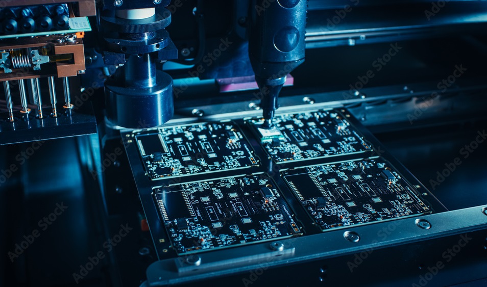
Before the hole metallization, the surface of the flexible PCB needs to be cleaned and polished to improve the bonding force between the hole metallization coating and the substrate. At the same time, the copper surface is effectively treated before the pattern imaging after the hole metallization. It is also important to strengthen the adhesion between copper foil and the etching layer. If the surface of the FPC board hole is not cleaned before metallization, the hole metallization coating may appear delamination and blistering. If the copper surface is not cleaned and roughened enough before the image is imaged and the bonding force is not enough, and defects such as seepage and short circuit are likely to occur in the subsequent electroplating process when making fine circuit patterns, which will cause the board to be scrapped.
In the method of grinding and roughening the surface of the copper clad laminate before hole metallization and pattern transfer, it is recommended to use alumina-containing abrasive 800#+1200# nylon needle brush roller, which can not only effectively remove the copper-plated particles, but also can effectively roughen the copper surface. The wear scar is controlled at 8-12mm, which can effectively prevent the board from being stretched due to excessive grinding and rolling. When processing the copper surface, the nylon needle wire containing alumina abrasive has a smaller cutting force than traditional silicon carbide abrasives. It can reduce the scratches on the board surface. The denser and finer the scratches, the better the bonding force between the board surface and the resist layer. We recommend to use wet pasting in the subsequent resist pasting to further enhance the bonding force between the board surface and the resist layer.
The chemical cleaning method is to use chemicals to remove organic impurities and organic pollutants on the surface, and then roughen the surface with a microetching solution. The surface of the copper plate after the treatment has good flatness, and there are no mechanical scratches and residual abrasive particles. Therefore it is an ideal cleaning and roughening surface treatment method in the processing of fine wire printed boards. However, this method is not easy to completely level the copper particles and foreign matter when removing the surface of the copper foil, and it is easy to oxidize and the roughness is not as good as the mechanical grinding effect. It is suitable for the treatment process before the covering film is applied.
Flexible printed boards are a fast-growing industry in China. Many materials and equipment still need to be explored continuously. Mass production also requires continuous completeness in the fields of technology, machinery and equipment, and materials. This article extracts a part of it that affects the quality of flexible boards. Only by mastering the essentials of each part can we produce products with higher performance, more reliability, and more beautiful appearance, and continue to grow the flexible printed board industry.


XPCB Limited is a premium PCB & PCBA manufacturer based in China.
We specialize in multilayer flexible circuits, rigid-flex PCB, HDI PCB, and Rogers PCB.
Quick-turn PCB prototyping is our specialty. Demanding project is our advantage.
Tel : +86-136-3163-3671
Fax : +86-755-2301 2705
Email : info@x-pcb.com
© 2024 - XPCB Limited All Right Reserve