- +86-755-23012705
- Building 3, Jinfeng Industrial Park, Fuyong Street, Baoan District, Shenzhen ,China
- [email protected]
Printed Circuit Board Assembly (PCBA) is at the heart of modern consumer electronics, connecting and powering the multitude of components that make our devices functional. As consumer electronics evolve, they demand more advanced, efficient, and compact designs. These requirements, in turn, place increasing pressure on PCBA processes and designs, driving innovation across the entire electronics manufacturing industry. In this blog, we will explore the impact of consumer electronics on PCBA processes and design, and how manufacturers are responding to these challenges and opportunities.
One of the most significant trends in consumer electronics is the drive toward smaller, more compact devices. Whether it’s the shrinking size of smartphones, wearables, or laptops, consumers expect electronics to be both portable and powerful. This miniaturization has had a profound impact on PCBA design and manufacturing processes.
To accommodate smaller form factors, PCBAs must fit more components into less space. This often requires the use of smaller components, such as microchips, miniature capacitors, and resistors. The components must also be arranged more efficiently to ensure they don’t interfere with one another’s function.
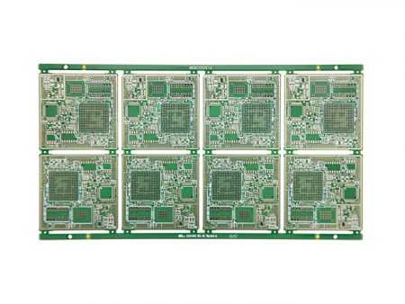
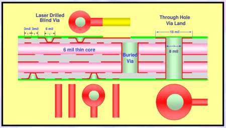
As a result, high-density interconnects (HDI) are commonly used in PCBA design to maximize the amount of circuitry in a smaller area. HDI PCBs feature finer trace widths, smaller vias, and multi-layer designs that allow for more connections in less space. However, this level of complexity demands precision in both the design and manufacturing processes. The challenges include maintaining signal integrity, ensuring the reliability of solder joints, and managing heat dissipation in a compact environment.

Consumer electronics are evolving to handle much higher levels of data processing and faster communication. From 5G-enabled smartphones to high-performance gaming consoles and AI-powered devices, the demand for high-speed data transmission has grown exponentially. This has had a significant impact on the design of PCBAs, which must now support high-speed circuits and fast data rates without compromising performance.
In response, signal integrity has become a primary focus in PCBA design. High-frequency signals are highly susceptible to interference, noise, and attenuation, which can affect the device’s performance. To mitigate these issues, engineers use advanced techniques such as:
Controlled impedance routing: Ensuring that signals travel along paths with a consistent impedance to reduce reflections.
Differential pair routing: Keeping signal pairs tightly together to minimize electromagnetic interference (EMI).
High-speed materials: Using materials with low dielectric loss to ensure signals are transmitted without degradation.
As consumer electronics demand faster processing speeds and more complex capabilities, PCBAs are designed to be thinner, lighter, and capable of handling these high-speed requirements. The added complexity requires more advanced manufacturing technologies, such as precision soldering and automated optical inspection (AOI), to detect even the slightest defects in high-speed circuits.
With the increasing power of consumer electronics comes the inevitable challenge of heat generation. Devices like smartphones, laptops, and gaming consoles house powerful processors, memory units, and graphics cards, all of which generate significant heat during operation. Without proper thermal management, this heat can damage components or reduce the lifespan of the device.
In response, thermal management has become a key consideration in PCBA design. To keep components cool, PCBAs must incorporate features like:
Thermal vias: Small holes in the PCB that allow heat to pass from one layer of the board to another, facilitating heat dissipation.
Heat sinks: Attachments to components like processors that help dissipate heat more effectively.
Copper layers: More copper layers in the PCB design help spread heat and reduce hotspots.
As consumer electronics become more powerful, it’s not enough to simply add larger heat sinks or increase the number of thermal vias. Manufacturers are exploring advanced materials and designs to maximize heat dissipation while minimizing the space required, ensuring devices remain sleek and functional. The challenge is to balance thermal performance with the compactness and lightweight design that consumers demand.
Another defining trend in consumer electronics is the increasing integration of smart features and connectivity. Devices are no longer just standalone tools; they are interconnected systems that communicate with other devices via Wi-Fi, Bluetooth, 5G, and other wireless protocols. The inclusion of features like voice assistants, IoT capabilities, and smart sensors further drives the complexity of the PCBA design.
For example, a modern smartphone’s PCBA not only needs to handle the basic functions of processing and storage but also needs to accommodate various communication modules, sensors (like GPS, accelerometers, and cameras), and power management systems. This requires multi-functional PCBAs capable of supporting various components with different electrical requirements and functions.
Additionally, the demand for seamless connectivity places emphasis on signal routing and electromagnetic compatibility (EMC). PCB designers must ensure that different modules do not interfere with one another while maintaining optimal signal quality. To meet these demands, PCBAs are often designed with shielding to prevent signal interference and improve the overall reliability of connected devices.

As environmental concerns grow, consumers are increasingly aware of the ecological impact of their electronics. As a result, manufacturers are under pressure to make PCBAs more sustainable, from using eco-friendly materials to reducing e-waste. The growing demand for sustainable electronics has led to significant changes in PCBA design and manufacturing practices.
The shift toward lead-free soldering has become one of the most prominent changes in recent years. Lead, a harmful substance, has been phased out in favor of lead-free solder alloys like tin-silver-copper (SAC) to comply with regulations like the European Union’s RoHS (Restriction of Hazardous Substances) directive. Additionally, manufacturers are adopting more recyclable materials for PCBs, such as biodegradable resins and non-toxic coatings.
The challenge for PCBA manufacturers is to balance sustainability with performance. For example, lead-free solders may have slightly different properties compared to traditional lead-based solders, which can affect the overall reliability of the assembly. Therefore, manufacturers must conduct extensive testing and adopt new processes to ensure that sustainability goals do not come at the cost of product quality.
While consumers demand increasingly advanced and feature-rich devices, they also expect them to be affordable. This presents a challenge for PCBA manufacturers, who must meet high-performance and high-quality standards while keeping costs in check. The competitive nature of the consumer electronics market means that manufacturers are under constant pressure to reduce production costs without compromising the performance of their PCBAs.
To achieve cost-efficiency, many companies are adopting surface-mount technology (SMT), which allows for faster, more automated assembly compared to traditional through-hole technology. SMT enables smaller, lighter, and more compact designs while reducing labor costs in the assembly process. However, as PCBAs become more complex and dense, manufacturers must invest in more sophisticated machinery and automation to maintain the required precision.

The demands of modern consumer electronics are reshaping the way PCBAs are designed and manufactured. As devices become smaller, faster, and smarter, PCBAs must evolve to meet the increasingly complex requirements of high-speed data, compact designs, and thermal management. At the same time, sustainability concerns and cost pressures add additional layers of complexity. To meet these challenges, the electronics industry is adopting new materials, advanced manufacturing techniques, and innovative design strategies.
As consumer electronics continue to evolve, the impact on PCBA processes and design will only grow. The future of consumer electronics is bright, and with it, the continued evolution of PCBAs will be critical to making these innovations a reality.
Simplify Your PCB Journey with XPCB Limited
XPCB Limited simplifies the PCB process for you. With our quick-turnaround prototyping and turnkey PCBA services, we ensure that your projects move forward smoothly and efficiently. Trust our commitment to quality and timeliness as we help you bring your designs to life. Choose XPCB Limited for a hassle-free PCB experience.


XPCB Limited is a premium PCB & PCBA manufacturer based in China.
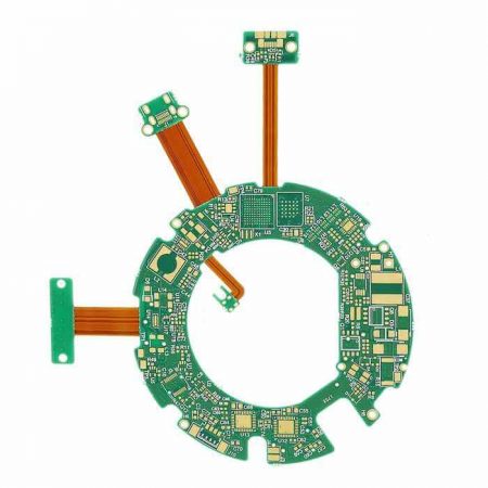
We specialize in multilayer flexible circuits, rigid-flex PCB, HDI PCB, and Rogers PCB.
Quick-turn PCB prototyping is our specialty. Demanding project is our advantage.
Tel : +86-136-3163-3671
Fax : +86-755-2301 2705
Email : [email protected]
© 2024 - XPCB Limited All Right Reserve
