- +86-755-23012705
- Building 3, Jinfeng Industrial Park, Fuyong Street, Baoan District, Shenzhen ,China
- [email protected]
Menu

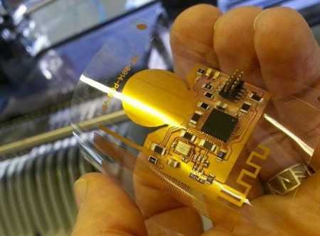
Because of their small size and size, there are few ready-made printed circuit board standards for the growing wearable Internet of Things market. Until these standards are available, we have to rely on the knowledge and manufacturing experience learned in board-level development and think about how to apply them to unique emerging challenges. There are three areas that require special attention: PCB base material, RF/microwave design, and RF transmission circuit.
PCB material:
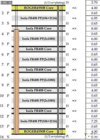
PCBs are generally composed of layers, which may be made of fiber-reinforced epoxy (FR4), polyimide, or Rogers material, or other laminated materials. The insulating material between different layers is called a semi-cured sheet.
Wearable devices require high reliability, so this becomes a problem when PCB designers are faced with the choice of using FR4(the most cost-effective PCB manufacturing material) or more advanced and expensive materials.
If wearable PCB applications require high-speed, high-frequency materials, FR4 may not be the best choice. The permittivity (Dk) of THE FR4 is 4.5, that of the more advanced Rogers 4003 series material is 3.55, and that of the younger Rogers 4350 series is 3.66.

The permittivity of lamination is the ratio of the capacitance or energy between a pair of conductors near the lamination to the capacitance or energy of a pair of conductors in a vacuum. At high frequencies PCB, it is desirable to have a small loss. Therefore, Roger 4350 with a dielectric coefficient of 3.66 is more suitable for applications at higher frequencies than FR4 with a dielectric constant of 4.5.
Under normal circumstances, the number of LAYERS of PCBs used in wearables ranges from four to eight. In the case of an 8-layer PCB, it should be able to provide enough layers and power supply layers with wiring layers sandwiched between them. In this way, ripple effects in crosstalk can be kept to a minimum and electromagnetic interference (EMI) can be significantly reduced.
In the circuit board layout design stage, the layout arrangement scheme is generally to place the large formation close to the power distribution layer. In this way, the ripple effect can be very low and the system noise can be reduced to almost zero. This is particularly important for the RF subsystem.
Compared with Rogers materials, FR4 has a higher dissipation factor (Df), especially at high frequencies. For higher performance FR4 laminates, the Df value is about 0.002, an order of magnitude better than ordinary FR4. But the Rogers lamination is 0.001 or less. When FR4 materials are used in high-frequency applications, there are significant differences in insertion loss. Insertion loss is defined as the power loss from point A to point B when using FR4, Rogers, or other materials.
Manufacturing problems
Wearable PCBS requires more stringent impedance control, which is an important factor for wearable devices, and impedance matching can result in cleaner signal transmission. In earlier times, the standard tolerance for signal-bearing routing was ±10%. This is clearly not good enough for today’s high-frequency, high-speed circuits. The current requirement is ±7% and in some cases ±5% or less. This parameter and other variables can seriously affect the manufacture of these wearable PCBs, which have particularly tight impedance controls, limiting the number of businesses that can manufacture them.
The permittivity tolerance of the stacking made of Rogers UHF material is generally maintained at ±2%, and some products can even reach ±1%, while the permittivity tolerance of the FR4 stacking is as high as 10%. Therefore, the comparison of these two materials shows that Rogers interpolation loss is particularly low. The transmission loss and insertion loss of Rogers laminates is 50% lower than that of conventional FR4 materials.
In most cases, the cost is the most important. However, Rogers can provide relatively low loss high-frequency lamination performance at an acceptable price. For commercial applications, Rogers can be combined with an epoxy-based FR4 as a hybrid PCB, with some layers made of Rogers material and others made of FR4.
Frequency is the primary consideration when selecting Rogers laminates. PCB designers tend to select Rogers materials when frequencies exceed 500MHz, especially for rf/microwave circuits, because the wiring above is strictly controlled by impedance, and these materials can provide higher performance.
Rogers materials also provide lower dielectric loss than FR4 materials, and their dielectric constant is stable over a wide frequency range. In addition, Rogers materials provide the ideal low insertion loss performance required for high-frequency work.
The thermal expansion coefficient (CTE) of Rogers 4000 series materials has excellent dimensional stability. This means that the thermal expansion and contraction of the circuit board can be maintained at a stable limit at higher frequencies and higher temperatures when the PCB goes through cold, hot, and very hot reflow cycles compared to FR4.
In the case of hybrid lamination, Rogers and high-performance FR4 can be easily mixed using common manufacturing process techniques, and thus relatively easy to achieve high manufacturing yield. Rogers lamination does not require a special through-hole preparation process.
Ordinary FR4 does not achieve very reliable electrical performance, but high-performance FR4 materials do have good reliable properties, such as higher Tg, are still relatively low cost and can be used in a wide range of applications, from simple audio design to complex microwave applications.
Rf/Microwave design considerations
Portable technology and Bluetooth pave the way for rf/microwave applications in wearable devices. Today’s frequency range is becoming more and more dynamic. Only a few years ago, very high frequency (VHF) was defined as 2GHz~3GHz. But now we can see UHF applications in the 10GHz to 25GHz range.
Therefore, for wearable PCB, the rf part needs to pay close attention to the wiring issues, and separate the signals separately, so that the wiring that generates high-frequency signals is far away from the ground. Other considerations include the provision of bypass filters, sufficient decoupling capacitors, grounding, and the design of transmission lines and return routes to be nearly equal.
The by-pass filter can suppress the noise content and the ripple effect of crosstalk. The decoupling capacitor needs to be placed closer to the pin of the device carrying the power signal.
High-speed transmission lines and signal circuits require a layer between the power layer signals to smooth the jitter caused by noise signals. At higher signal speeds, very small impedance mismatches result in unbalanced transmission and reception of signals, resulting in distortion. Particular attention must therefore be paid to impedance matching problems associated with rf signals, which have high speeds and special tolerances.
Rf transmission lines require controlled impedance to transmit rf signals from a specific IC substrate to a PCB. These transmission lines can be implemented in the outer, top, and bottom layers, or designed in the middle layer.
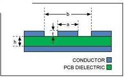
Methods used during THE PCB RF design layout include microstrip lines, suspended strip lines, coplanar waveguides, or grounding. The microstrip line consists of a fixed-length metal or line and a whole or part of the ground plane directly below. Generally the characteristic impedance of microstrip line structure from 50Ω to 75Ω.

Suspension strip lines are another method of wiring and noise suppression. The line consists of fixed-width wiring in the inner layer and a large ground plane above and below the center conductor. The ground plane is sandwiched between the power layers, thus providing a very effective grounding effect. This is a preferred method for wearable PCB rf signal routing.
Coplanar waveguides provide better isolation near rf lines and lines that need to be run close to each other. The medium consists of a central conductor and a ground plane on either side or below. The best way to transmit rf signals is by suspending strip lines or coplanar waveguides. These two methods provide better isolation between the signal and the RF routing.
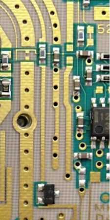
The so-called “through-fence” is recommended for both sides of the coplanar waveguide. This method provides a row of grounding through-holes in each metal ground plane of the central conductor. The mainline running in the middle is fenced on each side, thus providing a shortcut for the return current to the lower strata. This method can reduce the noise level associated with the high ripple effects of RF signals. The permittivity of 4.5 remains the same as that of the semi-cured sheet FR4 material, while the permittivity of the semi-cured sheet — from the microstrip line, strip line, or offset stripline — is about 3.8 to 3.9.

In some devices that use the ground plane, blind holes may be used to improve the decoupling of power capacitance and provide a shunt path from the device to the ground. The shunt path to ground reduces the length of the through-hole, which serves two purposes: you not only create the shunt or ground, but you also reduce the transmission distance of devices with small plots, which is an important factor in RF design.


XPCB Limited is a premium PCB & PCBA manufacturer based in China.
We specialize in multilayer flexible circuits, rigid-flex PCB, HDI PCB, and Rogers PCB.
Quick-turn PCB prototyping is our specialty. Demanding project is our advantage.
Tel : +86-136-3163-3671
Fax : +86-755-2301 2705
Email : [email protected]
© 2023 - XPCB Limited All Right Reserve
