- +86-755-23012705
- Building 3, Jinfeng Industrial Park, Fuyong Street, Baoan District, Shenzhen ,China
- [email protected]
Menu
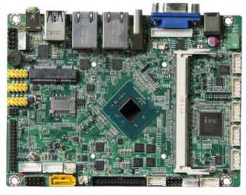
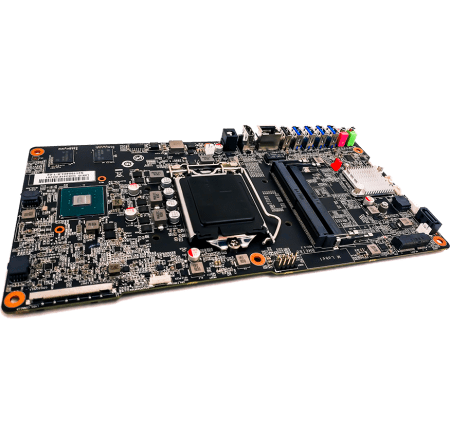
PCB assembly is the process of combining a circuit board with other electronic components such as connectors, housings, heat sinks, etc., to embed a product.
PCB Assembly Design: It is to consider PCB assembly in the early design stage to get a better product. A common problem for newbies is that the board is not designed with assembly in mind. More attention is paid to the PCB itself, and there is no understanding of the problems of the circuit board in the manufacturing process.
Individually, the PCB design may be okay and implementable, but there may be big mistakes in the later assembly, such as the components being too close to each other, the follow-up products may not work, or performance problems. The availability of components, if the components are not available, the entire manufacturing process will be delayed. So how do we avoid making these mistakes in general?
If you think about PCB assembly design, here are some PCB assembly design tips for you.
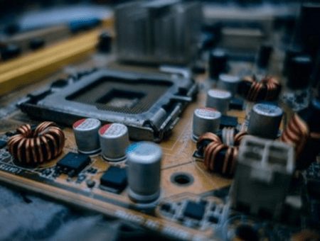
Two components that are too close to each other can interfere with each other and cause problems. At that point, redesign and manufacturing may be required, resulting in a loss of time and money. When there are enough gaps between component boundaries, the potential problems caused by components being too close together can be reduced.
When placing components, it is important to prevent component shapes from overlapping each other, and generally speaking, routing and layout rules require that discrete components such as capacitors and resistors be spaced at least 10 mils, with 30 mils being the preferred spacing. There are some other spacing rules, as shown below.

This better ensures that there isn’t much conflict between the design and the actual assembly. Smaller components usually take up less space on the PCB, so consider whether you can reduce the size of the component to create more space on the PCB.
Lead-free components should not be mixed with lead-containing components, and if any component requires lead-free assembly and no standard lead adhesive is available, the entire PCB, including the components, must be assembled lead-free.
Sometimes, the package available for a particular device is a lead-free BGA, but there are usually some specific requirements. When PCB fabrication and assembly are not tightly coordinated, there are separating pieces left between the PCBs after wiring that interfere with the assembly of connectors that also extend to that edge.
Distribute large components as evenly as possible on the PCB during the layout process to achieve better heat distribution during reflow. Make sure the PCB vendor has a reflow profile for the amount of reflow.
Avoid mixing techniques as much as possible. If you use plug-ins, try to place them on the same side of the board as possible, which can reduce the cost and time of PCB manufacturing and assembly.

Mechanical drilling like 6 mil is very small and is not recommended unless there is no other option. Due to the BGA density, 18.5/8 (18.5mil pad/8mil drilling) is recommended, ideally, 22/10 would be fine, but BGA does not allow it.
The components used in the design should be double-checked early in the layout process, and if there is space on the board and the current design uses unnecessary widgets, the designer may recommend a larger component. This will help avoid multiple processes in the assembly process. For example, if possible, use a resistor of 0805 instead of a resistor of 1206. If the resistor of 0805 is sufficient, then the resistor of 1206 will not be chosen, which will reduce the size of the PCB.
The availability of components can lead to significant delays, so it is necessary to check the inventory, delivery date, and discontinuation of components at the design stage.
The bill of materials (BOM) is a critical aspect of design and assembly.If there are any issues in your BOM, the PCB fab will pause the project until the issue is resolved with the engineer.One way to ensure that the BOM is updated is to review the BOM at any time when the design changes.
When you add new components to your schematic during the layout process, make sure you also update the BOM with the correct part numbers, descriptions, and assembly values. During the design process, engineers may change components due to long lead times, dimensions, or availability, and forget to update the BOM with a new part number. This can lead to various assembly issues and cause delays.

Nowadays, many PCB factories are one-stop, PCB board design, material procurement, stencil fixture, and PCB assembly are all together. But if your components aren’t all supplied by the PCB fab, you’ll have to provide the parts in a well-organized kit that matches the BOM. The required SMT components must be supplied in rolls, or in the form of continuous tape that is at least 6 inches long, or in the form of tubes or trays.
Component footprint is another major aspect of layout design. It is important to correctly use the number keys in the datasheet to identify the correct part and its pad pattern. Reading the datasheet incorrectly can result in an incorrect footprint, which may require a complete redesign and remanufacturing of the PCB.
Each connection of each component must have its own separate pad. Each pad should be sized to match its mating pieces. If two components share a single pad, say, a resistor and a capacitor, neither will be properly aligned during assembly.

One important way to ensure that your PCB is error-free and works seamlessly is to run design for manufacturing (DFM) tests. This test identifies most errors in the design at an early stage, avoiding costly errors and delays at a later stage. Problems such as spacing, component polarity, and package verification can be well identified in a timely manner.
Simplify Your PCB Journey with XPCB Limited
XPCB Limited simplifies the PCB process for you. With our quick-turnaround prototyping and turnkey PCBA services, we ensure that your projects move forward smoothly and efficiently. Trust our commitment to quality and timeliness as we help you bring your designs to life. Choose XPCB Limited for a hassle-free PCB experience.


XPCB Limited is a premium PCB & PCBA manufacturer based in China.
We specialize in multilayer flexible circuits, rigid-flex PCB, HDI PCB, and Rogers PCB.
Quick-turn PCB prototyping is our specialty. Demanding project is our advantage.
Tel : +86-136-3163-3671
Fax : +86-755-2301 2705
Email : [email protected]
© 2023 - XPCB Limited All Right Reserve
